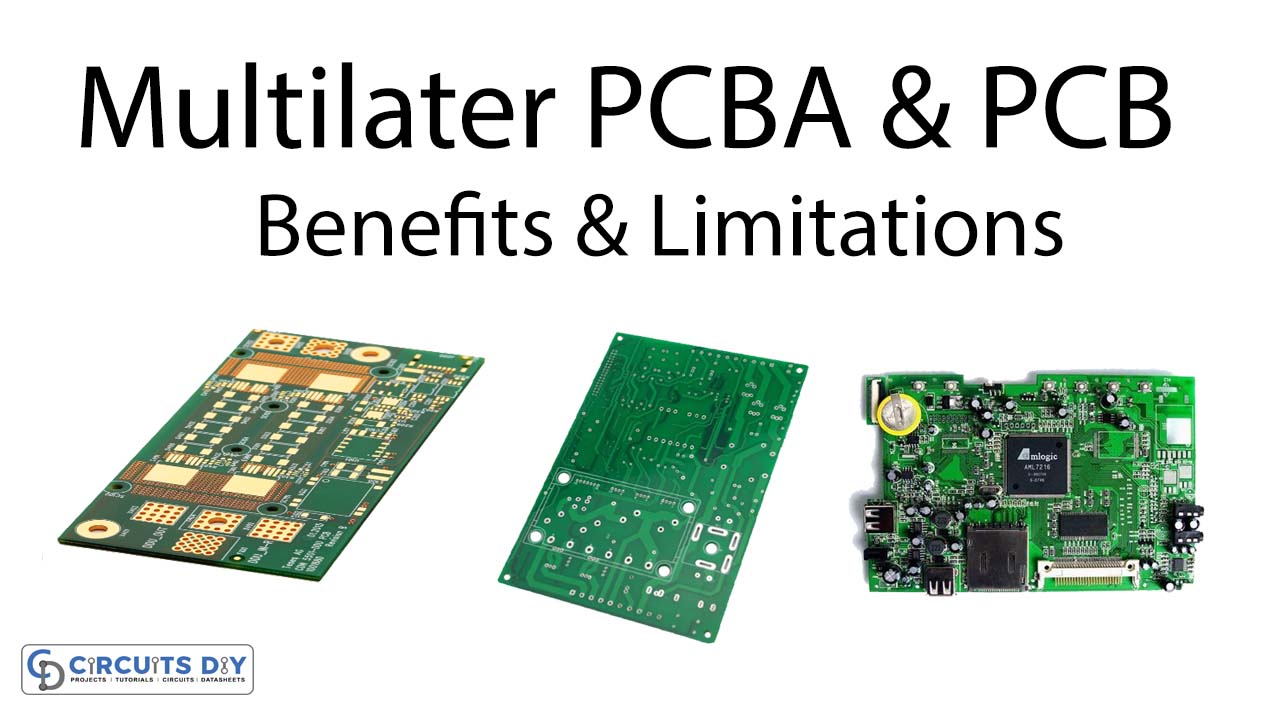
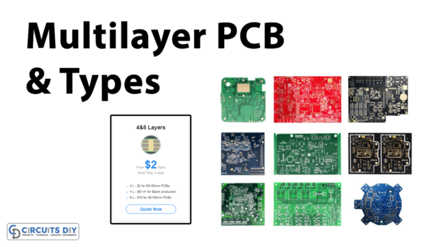
With the ever-increasing design complexity & miniaturization of technology size in healthcare, military, and industrial applications. The demand for high-grade Multilayer PCBA has increased ten folds over the decade. Smartphones & PCs perfectly represent applications for multilayer PCBA with their need for compactness, yet sophisticated functionality. So, In this guide will take a deep dive into the pros and cons of incorporating Multilayer PCBA into your projects & how you can determine if you really need to go for a multilayer PCB in order to fulfill your design needs. FS Tech is a multilayer PCB Assembly Manufacturer in china.
What are Multilayer PCBs?
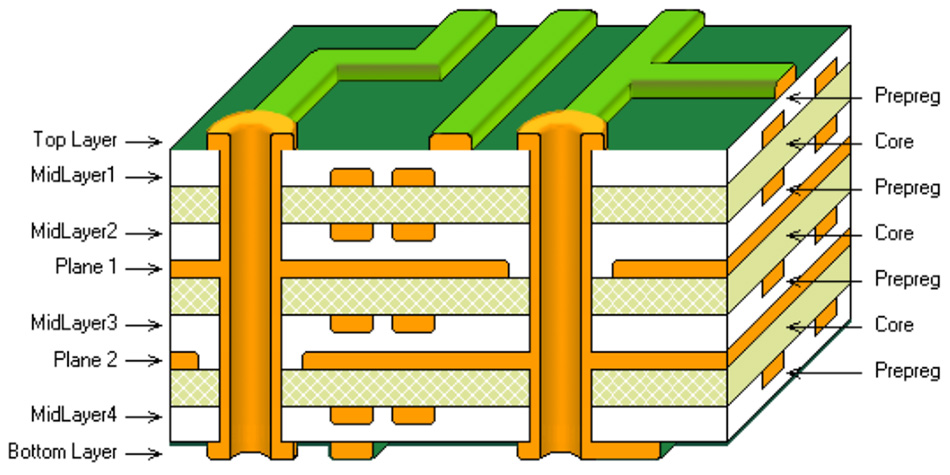
Simply speaking, A Multilayer PCB is a class of PCB that consists of 3 or more conductive copper foil layers. It generally appears as many layers of a double-sided circuit board, laminated and glued together with various layers of heat-protective insulation between them. A conductive pathway is etched on both sides for connecting different components. All circuit connections among the layers are done using vias such as plated through holes, blind, and buried vias.
Technical Benefits of Using Multilayer PCBA

1) Increased Durability
The process involved in making multilayer PCBs subjects them to high temperatures & pressure which allows them to be more durable than the common PCB boards Also, Not only does a multilayer PCB has to withstand its own weight, but it must also be able to handle the heat and pressure used to bind the incorporated layers together.
2) Reduced Weight
The small size of the PCB ultimately reduces its overall weight of the PCB. So multilayer PCBs are usually lightweight, very portable, and can be used in handheld electronics.
3) Single Point Connection
Since multilayer PCBs work as a single unit, they all have a single one-point connection. This proves to be very beneficial in consumer electronic product design since the designer only needs to include a single connection point in the final product.
4) Enhanced Layout Density
PCB board density has a directly proportional relationship to the number of components per unit size of PCB. Considering this, Multilayer PCBs have an inherent advantage of being able to accommodate a higher number of onboard components as compared to a generic single-layer PCB.
5) Easy To Install
Due to their small size & reduced weight, multilayer PCBs are easy to install in complex machinery & cramped consumer electronics where it becomes difficult to allow a greater amount of clearance without hurting the user experience.
Design Limitations Or Cons of Using Multilayer PCBA
1) Expensive To Design
Multilayer PCBs are essentially more costly than single and two-fold layer PCBs at each phase of the assembling cycle. They are hard to configure, setting aside a broad measure of effort to work out any possible issues. They also require a highly complex manufacturing process to produce, which takes a great deal of time and labor on the part of assembly personnel.
2) Requires an Intricate Production Process
Due to being complex in nature, multi-layer PCBs need a higher production time and more thought-out manufacturing techniques than other PCB types. This is because even a single mistake in the design process can turn a perfectly functional PCB into scrap metal.
3) Sparse Availability
This is a very common issue that occurs when designers decide to use multilayer PCBs for their assignments. Producing Multilayer PCBs requires complex machinery that is usually very expensive. Not all PCB manufacturers have the funds or the necessity for this machinery, so not all PCB manufacturers carry it. This limits the number of PCB manufacturers available to produce multilayer PCBs for clients.
4) Longer Production Times
Since this kind of PCB is harder to make, therefore they require a longer production time. This can cause issues for some designers who operate on a tight schedule.


