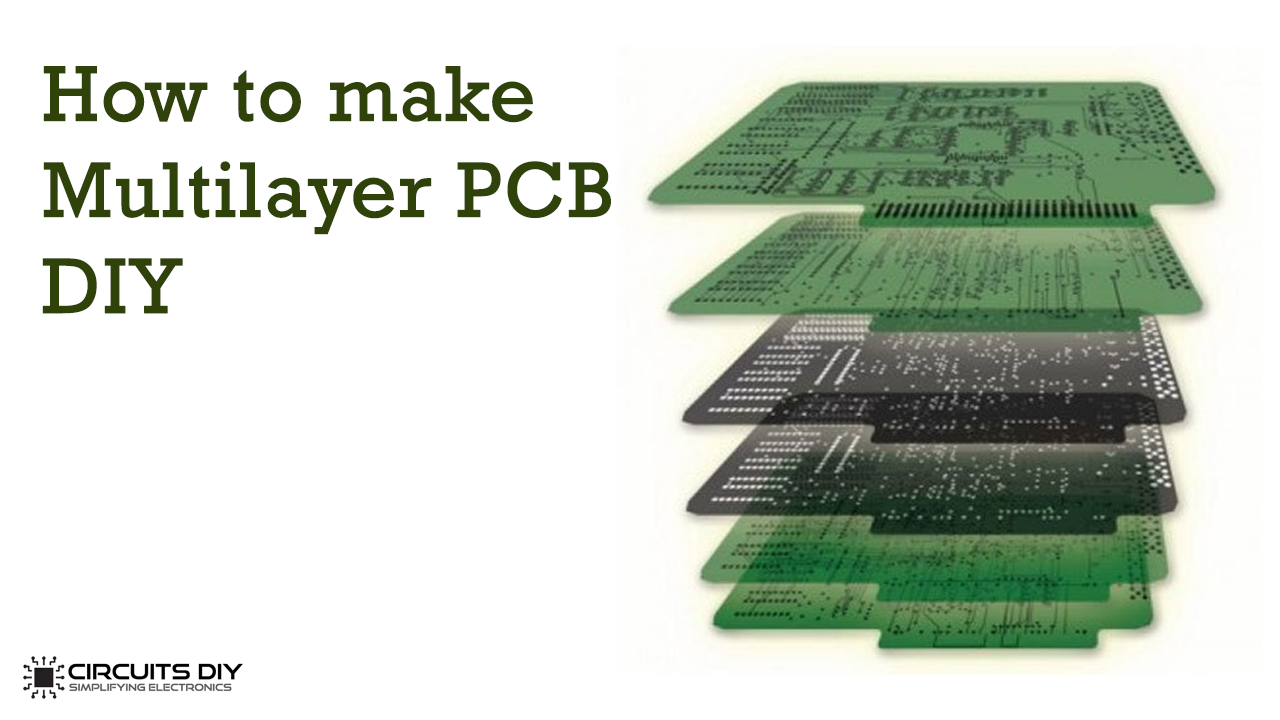
What is a Multilayer PCB?
PCBs or printed circuit board technology is imperative for modern-day electronics, whether it be building a simple homemade electronic project or performing technology size reduction for complex industrial processes. PCBs have become a vital part of nearly every product development cycle. So, in this article, we are going to go over a step by step process on how to How To Make A Multilayer PCB At Home.

To Buy Custom built PCB’s at Low prices please visit: www.pcbway.com
A Multilayer PCB is a class of PCB that consists of 2, 3, or more conductive copper foil layers. It generally appears as many layers of a double-sided circuit board, laminated and glued together with various layers of heat-protective insulation between them. A conductive pathway is etched on both sides for connecting different components. All circuit connections among the layers are done using vias such as plated through holes, blind and buried vias.
Equipment Required For Multilayer PCB
You will need the following parts to build this project.
| S.No | Component | Value | Qty |
|---|---|---|---|
| 1) | Copper Clad Board w/ Fiber sheet Base | 100x70mm | 1 |
| 2) | Glossy Photo paper | – | 1 |
| 3) | Rubbing Alcohol | – | 1 |
| 4) | Acetone | – | 1 |
| 5) | Flat Iron (In case you want to use heating method for circuit transfer) | – | 1 |
| 6) | Ferric Chloride (FeCl3) | – | 1 |
| 7) | Etching Tray | – | 1 |
| 8) | Utility Knife | – | 1 |
| 9) | Scratch Pen | – | 1 |
| 10) | Masking Ink / Epoxy w/ oil color | – | 1 |
| 11) | Solid Ink Printer | – | 1 |
| 12) | Laptop/PC (with a prepared PCB design) | – | 1 |
| 13) | Hand Drill w/ drill bits | 3.2mm – 8mm drill bits | 1 |
Useful Steps For Making Multilayer PCB
Follow each step carefully as described below:
1) Get All Your Tools in Order
Before starting the process get all your tools in order. Ensure the use of a copper-clad board with a Fiber Sheet Base, as the base idea behind this DIY is to use them as a base. Also, get your PCB schematic printed on a glossy photo paper.
2) Separate Fiber Sheets From Copper Clad
Using the utility knife peel of all the fiber sheets attached with the copper clad one by one. There will be a number of fiber sheets attached to the base of the copper clad & you will need to separate all them one by one, leaving only the last one with the copper clad.

3) Slice up & Clean the Copper Clad
Cut as much as the layers of the same size you require from the copper-clad and keep them apart as mentioned above.
4) Transfer of Circuit to Copper Clad Using a Heating Element or Heatless Toner Transfer Method

Print your PCB schematic onto a glossy photo paper using a solid ink printer. Now, the next step is to transfer the printed PCB schematics on the copper clads. Here 2 methods are applicable, you may use the one best suited to your needs.
To Buy Custom built PCB’s at Low prices please visit: www.pcbway.com
Heating Element Toner Transfer Method
In this method you basically iron the printed circuit on the copper-clad using a heating element such as a flat iron. laundry iron usually works best. Ironing transfers the ink from the photo paper & fuses it to the PCB board. If the paper is very thick, set the iron to the highest possible setting or to the medium setting if not.
Heatless Toner Transfer Method
First clean the copper clad using freshwater & a tissue. After that, use a good amount of Alcohol & Acetone mixture in an 8:3 ratio on the copper clad. Then place the photo paper over it. The entire paper should cover the Alcohol-acetone coated copper clad in one go. Let it dry for 30 min, after which dip the board in some freshwater before peeling the photo paper. Carefully start the peeling processing, letting the board dry for a couple of minutes in case you see pieces of paper sticking to the board. After the peeling off the photo paper, remove any residual paper by using a tissue.
5) Etching
Place the Cu clads in the ferric chloride (FeCl3) solution for around 5-8 minutes. The time for etching will depend on the levels of temperatures and the thickness of the copper sheet. After this check the traces & remove any unwanted copper between the traces using a scratch pen.

6) Aligning & Securing the Copper Clads
Align each copper sheet precisely & secure them together using 5 min epoxy glue. Let it dry for a couple of minutes and clean it using Acetone or any other cleaner. Sand the board to remove any residual glue.
7) Apply Masking Ink & Drill Vias
One the etching is done & you glued all the layers together, It is time to define the traces using masking ink & a stencil or Two-part epoxy with oil colors. After the traces are defined, drill the vias using a hand drill & solder all the pads & vias by using thin wire among the layers.

Advantages of Multilayer PCB
- Multilayer PCBs are inherently light-weight & easy to work within complex machinery & yields higher mobility.
- Being high-density assemblies, multilayer PCBs are very powerful. Merging multiple layers into a single PCB allows the board to be more connective, improves speed allows to achieve greater component capacity.
For Cheap PCB Prototypes under 5$ please visit: www.pcbway.com
See Also: DIY Flex PCBs | PCB Soldering For Beginners | Do’s & Dont’s of PCB Routing
Related posts:
 PCB Manufacturing: Step By Step Process
 How To Build the PCB Best - JLCPCB
 Complete PCB Designing Tutorial Using EasyEDA PCB Design Tool
 Multilayer PCBA & PCB | Benefits And Limitations Over Conventional PCB
 Copper Clad Laminate (CCL) | Comprehensive Guide For Beginners
 Printed Circuit Boards in Different Industries


