
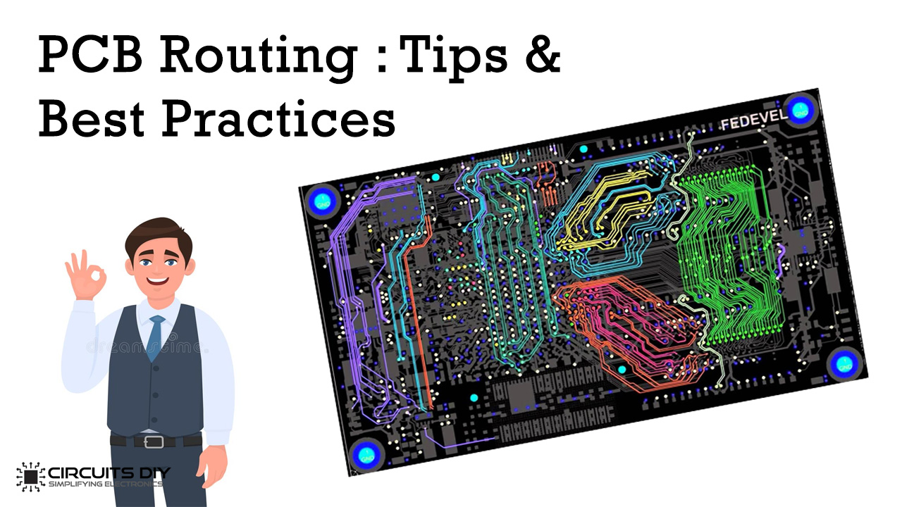
Printed circuit board (PCB) design brings electronic circuits to life. Through the use of a layout software, the PCB design process combines component placement and routing to define electrical connectivity on a manufactured circuit board. Nowadays, Electronic devices are regularly shrinking due to consumer demands for portability and light-weight products such as big-screen televisions, tablet computers, and powerful smartphones, drone devices and recently, even wearable technology. So, in this article, we will go through a complete Beginners guide to PCB routing & will take a look at some of the top tips and best practices you can use to take your PCB routing skills to the next level.
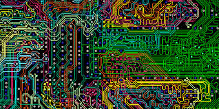
The PCB routing process is both an art and a science. Using physical wires, you define the electrical connectivity between components on a PCB layout. No two circuit boards are the same, the routing is what makes your design unique. Poor PCB Routing can lead to function and reliability problems. So, let’s jump right into this Beginners Guide To PCB Routing & go through some of the top tips and best practices to guide you through the intricate process of PCB routing.
PCBWay commits to meeting the needs of its customers from different industries in terms of quality, delivery, cost-effectiveness, and any other demanding requests. As one of the most experienced PCB manufacturers in China. They pride themselves to be your best business partners as well as good friends in every aspect of your PCB needs.
1) Choice of PCB Design Software Matters
One of the biggest mistakes many beginners make is choosing the wrong PCB design software. The choice of PCB design software matters, but don’t rely too much on their self-correcting features. If you are looking for a great user-friendly PCB Design software package for beginning electronic designers then click here.
2) Auto-routing Is Not Always Accurate!
Auto-routing is a useful tool and as a beginner, you may use it frequently thinking of it as an easy way to solve your routing problems. but do not rely on it too heavily. Autorouters are often inaccurate and asymmetrical, therefore making them unreliable. You should do the routing manually to ensure quality and accuracy.
3) Proper Trace Widths Are Crucial
In order to ensure proper PCB routing and to avoid PCB cards with broken connections. It is very important to properly size your trace widths. When you have electricity running across all your copper traces, it’s going to produce a generous amount of heat. Controlling the width of your traces is one of many ways to reduce how much heat builds up on your board, and the wider your traces, the less resistance that electricity will encounter when flowing through your circuit.
4) Leave Room Between Traces
It is very important that you leave adequate space between all your PCB traces and pads. It reduces the risk of a short circuit developing when your board is finished and traces unintentionally connect. The general recommendation is to leave at least a gap of 0.007” – 0.010” of space in-between every adjacent traces and pad on the PCB.
5) Avoid 90° Trace Angles
Always avoid 90° trace angles, as they lead to shorts in the PCB card. When you have a bunch of traces with a 90° right angle turn on your board, the outside corner of that 90-degree angle has the likelihood of being etched narrower than your standard trace width. This can lead to inaccuracies in the final layout design leading to excessive heat generation within the narrow ridges of the trace. Use 45° trace angles instead.
6) Make Use of Vias
Ensure proper usage of vias. Vias are perfect for facilitating electrical connectivity between the separate layers on your board, as they transfer heat from one section of the board to the other, which is really useful when you have a component that draws a high amount of current on the board.
7) Width of Power & Ground Traces
The width of power and ground traces should greater than all other traces on the board. Because an excessive amount of current flows through them, and average trace width for power and ground traces may result in burning up of wires and board failure.
In Conclusion, by adhering to the above tips and best practices you can boost your PCB routing skills and avoid the common pitfalls which may pose a threat to your PCB designing process.
Related posts:
 How to Remove Printed Circuit Board (PCB) Corrosion
 Important Tools for Printed Circuit Board Designing
 Top 6 PCB Testing Techniques Involved in PCB Manufacturing
 Understand PCBA And Its Manufacturing Process
 PCB Design 101 - Top 5 Fatal Mistakes Made With PCB Designs
 Bad Solder Joints|Common PCB Soldering Issues and their Solution


2 thoughts on “Beginners Guide To PCB Routing: Tips & Best Practices”
Comments are closed.