
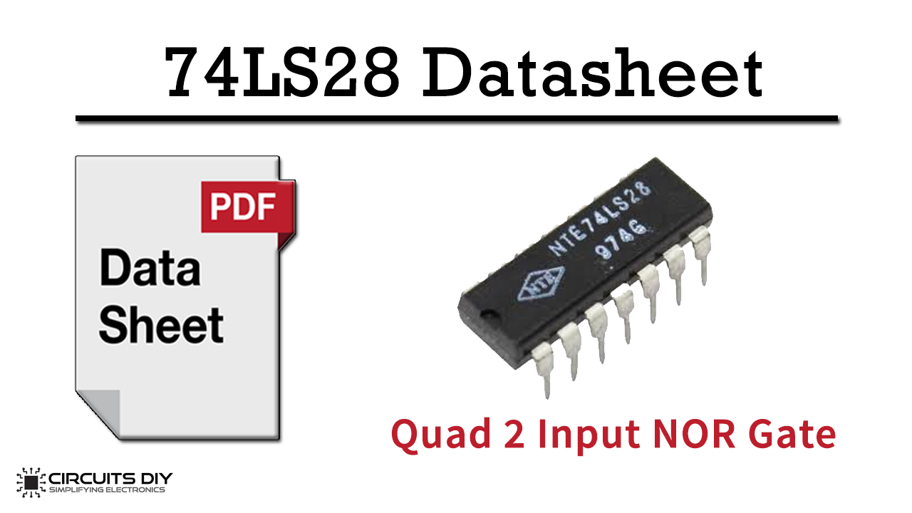
74LS27 IC is a member of the 74XXYY IC series. It has 4 (Quad) NOR gates in the chip and each gate have two inputs, hence the name Quad 2 – Input NOR Gate. The 74LS28 IC has a wide range of working voltage, a wide range of working conditions, and directly interfaces with CMOS, NMOS, and TTL. The output of the IC always comes in TTL which makes it easy to work with other TTL devices and microcontrollers. The IC 74LS28 is smaller in size and it has a much faster speed which makes it reliable in every kind of device.
What is NOR Gate?
An OR gate followed by a NOT gate in a cascade is called a NOR gate. The inclusive NOR (Not – OR) gate has an output that is normally at logic level “1” and only goes “LOW” to a logic level “0” when any of its inputs are at logic level “1”. The Logic NOR Gate is the reverse or complementary form of the inclusive OR gate.
74LS28 Key Features & Specifications
- Max Supply Voltage 5.5V
- Max Input Voltage 2V
- TTL outputs
- Maximum ESD: 3.5KV
- Operating voltage range: +4.75V to +5.25V
- Low power consumption
- Operating Free Air Temperature Range 0°C to +70°C
- Storage Temperature Range -65°C to +150°C
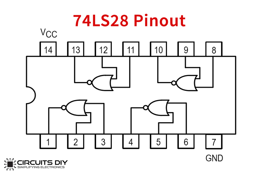
74LS28 Pinout
| Pin No. | Pin Name | Description |
|---|---|---|
| 1 | 1Y | Output of gate 1 |
| 2 | 1A | Input of Gate 1 |
| 3 | 1B | Input of Gate 1 |
| 4 | 2Y | Output of gate 2 |
| 5 | 2A | Input of Gate 2 |
| 6 | 2B | Input of Gate 2 |
| 7 | GND | Ground |
| 8 | 3A | Input of Gate 3 |
| 9 | 3B | Input of Gate 3 |
| 10 | 3Y | Output of gate 3 |
| 11 | 4A | Input of Gate 4 |
| 12 | 4B | Input of Gate 4 |
| 13 | 4Y | Output of gate 4 |
| 14 | Vcc | Chip Supply Voltage |
Aplications
The 74LS28 IC has a number of uses , some of them are listed as below:
- The IC can be used for Noise Removing.
- Also used in devices such as PCs and notebooks.
74LS28 Datasheet
You can download the 74LS28 IC Datasheet from the link given below:
See Also: 7407 Hex Buffer IC | 74LS08 Quadruple Two Input AND Gate IC | 74LS00 Quad Two Input NAND Gate
Related posts:
 2SC1047 NPN Small Signal Transistor - Datasheet
 LM2991 Adjustable Negative Low Dropout Voltage Regulator - Datasheet
 LM311 Voltage Comparator - Datasheet
 LT1014 Quad Precision Operational Amplifier
 LM1084 Adjustable 5A Low-Dropout Positive Regulator - Datasheet
 DF08M 800V 1A Full Wave Bridge Rectifier - Datasheet


