
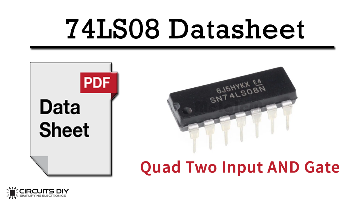
74LS08 Quadruple IC is a member of the 74XXYY IC series. There are four AND gates in the chip and each gate has two inputs, hence the name Quadruple 2- Input AND Gate. IC 74LS08 uses only one single power supply and it also comes in multiple packages to solve the requirement according to the circuit. The output of the IC always comes in TTL which makes it easy to work with other TTL devices and microcontrollers. The IC 74LS08 is smaller in size and it has a much faster speed which makes it reliable in every kind of device.
What is an AND Gate?
An AND Gate is a logical operator/circuit that gives a logical high (1) output only when all of its inputs are high (1), otherwise, it results in a logical low (0).
74LS08 Pinout
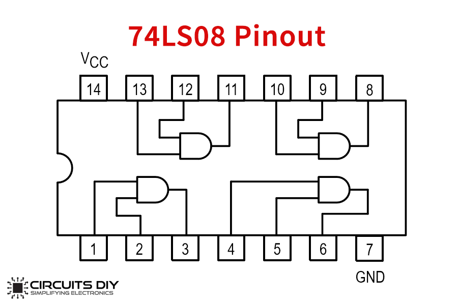
74LS08 Pin Configuration
| Pin No | Pin Name | Description |
|---|---|---|
| 1 | A1 | INPUT 1 of GATE 1 |
| 2 | B1 | INPUT 2 of GATE 1 |
| 3 | Q1 | OUTPUT of GATE 1 |
| 4 | A2 | INPUT 1 of GATE 2 |
| 5 | B2 | INPUT 2 of GATE 2 |
| 6 | Q2 | OUTPUT of GATE 2 |
| 7 | GND | Ground |
| 8 | A3 | INPUT 1 of GATE 3 |
| 9 | B3 | INPUT 2 of GATE 3 |
| 10 | Q3 | OUTPUT of GATE 3 |
| 11 | A4 | INPUT 1 of GATE 4 |
| 12 | B4 | INPUT 2 of GATE 4 |
| 13 | Q4 | OUTPUT of GATE 4 |
| 14 | VCC | Supply Voltage |
74LS08 Specifications
- Operating voltage range: +4.75 to +5.25V
- Recommended operating voltage: +5V
- Maximum supply voltage:7V
- Maximum current allowed to draw through each gate output: 8mA
- TTL outputs
- Low power consumption
- Typical Rise Time: 18ns
- Typical Fall Time: 18ns
- Operating temperature:0°C to 70°C
- Storage Temperature: -65°C to 150°C
74LS08 Applications
- The chip provides TTL outputs that are needed in some systems.
- 7408 IC is usually used in a place where a logical AND operation is required.
You can download this Datasheet for 74LS08 Quadruple from the link given below:
See Also: S8050 NPN Transistor | 74LS02 Quad Two Input NOR Gate | 74LS00 Quad Two Input NAND Gate


4 thoughts on “74LS08 Quadruple Two Input AND Gate – Datasheet”
Comments are closed.