
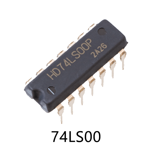
74LS00 is a member of the 74XXYY IC series. The 74LS00 is a TTL (Transistor to Transistor Logic) which uses low power Shottky transistors to reduce the stored charge and get higher switching speeds than with conventional bipolar transistors. 74LS00 is a 14 pin IC that has four NAND gates each NAND gate has two inputs & one output.
NAND Gate
In Digital Electronics NAND Gate is the logic gate which produces an output High (1) when all of its input are LOW (0).
74LS00 Features and Specifications
- Operating voltage range: +4.75 to +5.25V
- Maximum supply voltage:7V
- Maximum current allowed to draw through each gate output: 8mA
- TTL outputs
- Maximum ESD: 3.5KV
- Typical Rise Time: 15ns
- Typical Fall Time: 15ns
- Operating temperature:0°C to 75°C
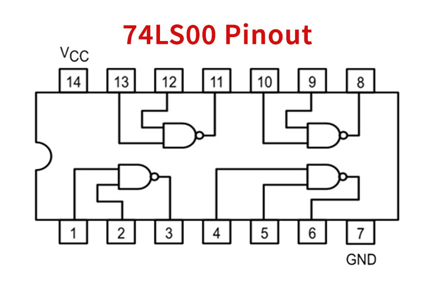
74LS00 Pin Configuration
| Pin No | Pin Description |
|---|---|
| 1 | A1-INPUT |
| 2 | B1-INPUT |
| 3 | Y1-OUTPUT |
| 4 | A2-INPUT |
| 5 | B2-INPUT |
| 6 | Y2-OUTPUT |
| 7 | GND |
| 8 | Y3-OUTPUT |
| 9 | A3-INPUT |
| 10 | B3-INPUT |
| 11 | Y4-OUTPUT |
| 12 | A4-INPUT |
| 13 | B4-INPUT |
| 14 | VCC |
74LS00 Pinout
Application
- 74LS00 basically used for performing NAND function
- Can be used as logic inverter
74LS00 Datasheet
Download 74LS00 Datasheet from the link given below.


3 thoughts on “74LS00 Quad Two Input NAND Gate – Datasheet”
Comments are closed.