
74LS07 Hex Buffer/driver features high-voltage open-collector outputs to interface with high-level circuits or for driving high-current loads. They are also characterized for their usage as buffers for driving TTL inputs.
A Hex buffer is a basic logic gate that passes its input, unchanged, to its output. Its behavior is the opposite of a NOT gate. The main purpose of a buffer is to regenerate the input, usually using a strong high and a strong low. A buffer has one input and one output; its output is always equal to its input. Buffers are also used to increase the propagation delay of circuits by driving the large capacitive loads.
74LS07 Pinout
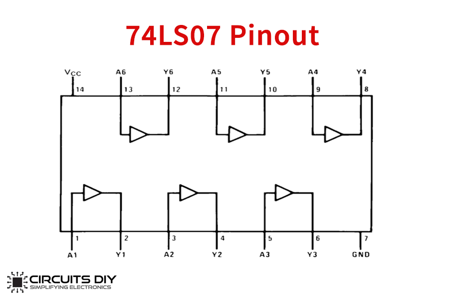
74LS07 Pin Configuration
| Pin No | Pin Name | Description |
|---|---|---|
| 1 | 1A | Buffer input pin 1 |
| 2 | 1Y | Buffer output pin 1 |
| 3 | 2A | Buffer input pin 2 |
| 4 | 2Y | Buffer output pin 2 |
| 5 | 3A | Buffer input pin 3 |
| 6 | 3Y | Buffer output pin 3 |
| 7 | GND | Ground |
| 8 | 4Y | Buffer output pin 4 |
| 9 | 4A | Buffer input pin 4 |
| 10 | 5Y | Buffer output pin 5 |
| 11 | 5A | Buffer input pin 5 |
| 12 | 6Y | Buffer output pin 6 |
| 13 | 6A | Buffer input pin 6 |
| 14 | VCC | Supply Voltage |
74LS07 Specifications
- Six Independent Hex Buffer Gates
- Open Collector Outputs Require Pull-Up Resistors
- Input Clamping Diodes
- Standard TTL Switching Voltages
- Supply Voltage 7V
- Input Voltage 5.5V
- Output Voltage 30V
- Operating Free Air Temperature Range 0°C to +70°C
- Storage Temperature Range -65°C to +150°C
Applications
The 74LS07 IC has a number of uses , some of them are listed as below:
- Convert TTL Voltage Levels to MOS Voltage Levels.
- High Sink Current Capability.
- Inputs Fully Compatible With Most TTL Circuits.
- Clamping Diodes at Input Simplify System Design.
- Open-Collector Driver for Indicator Lamps and Relays.
You can download this Datasheet for 74LS07 Hex Buffer IC from the link given below:
See Also: 74LS04 Single Input NOT Gate/Hex Inverter | 74LS02 Quad Two Input NOR Gate | 74LS00 Quad Two Input NAND Gate


7 thoughts on “74LS07 Hex Buffer with High Voltage Open-Collector Outputs – Datasheet”
Comments are closed.