
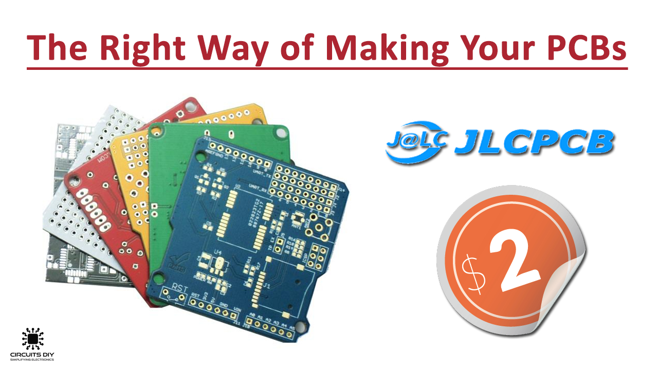
Learning new exciting hobbies & making them a part of our life is a part of human nature. Many people step into the domain of electronics due to the simple ” I can make this with my hands” analogy. Venturing within the realm of electronics, most hobbyists stumble upon the most intriguing & intricate way of designing electronic circuits known as PCBs. PCBs offer a wonderful possibility of designing a professional-looking circuit with the help of any CAD/CAM software & a small scale fab house. But as the circuit complexity & no. of projects increase, you’ll need a proper PCB manufacturer that can cater to all your design needs. One of the best names in the current PCB manufacturing market is JLCPCB. So, in this tutorial, we will see how you can design & order your next PCB using EasyEDA & JLCPCB.
What is JLCPCB?

JLCPCB is a worldwide leading PCB prototype enterprise and a high-tech manufacturer specializing in quick PCB prototype and small-batch PCB production. With over 14 years of experience in PCB manufacturing, JLCPCB has more than 800,000 customers. JLCPCB is a professional PCB manufacturer-featuring a large production scale, great manufacturing & production facilities, and superior PCB quality.
We are ever so thankful to our sponsors at JLCPCB for sponsoring projects on this website and YT channel. JLCPCB is the Best PCB prototype & manufacturing company in china, assuring the best service you will ever experience regarding (Quality, Price & Time). We strongly recommend you to order your next PCB from JLCPCB. For this, all you need to do is just download the Gerber file and upload it to the JLCPCB website after creating an account, visit their website to look for more!.
Ordering Your PCB Online Using JLCPCB
Following steps will show you how you can use JLCPCB services to order your next PCB online.
Step 1: Make Your PCB Design Using EasyEDA
First of all, draw the initial schematic of your PCB using the EasyEDA design tool. For this, Go to the EasyEDA website and create a free account. Registering using a Google Account is also possible Once you are logged in, Go to “Editor” and create a new project. Now start drawing your circuit diagram. Make sure you add the components from JLCPCB/LCSC library while drawing the schematics in EasyEDA.
To Buy Custom-built PCBs at amazingly low rates 2$ for 5 PCB’s Please visit the JLCPCB website
Step 2: Place & Route the Components
After that, search for the correct components from the library & place them on the canvas in EasyEDA using the “wire” tool. After the schematic is complete, verify & save the circuit.
Step 3: Design the PCB Layout
After that, go to the top tool list, Click on the convert button and select “Convert to PCB”. A new window with the PCB layout will open, where you can place the components inside the boundary and arrange them any way you want. In order to get the best possible look for your PCB, place & route parts with identical functions close to each other.
After placing all the parts as per your need, save the PCB layout. After saving, start the routing of your PCB components. You can use the manual routing tool to do this. But, an easier approach is to use the built-in autoroute feature. To use that, Click on the “Route” Tool and Select “Auto Router”. This will open an Auto Router Config Page where you can provide details such as clearance, track width, layer information, etc. Once you have done that, click on “Run”.
Step 4: Create & Download Gerber, BoM & CPL/PNP Files
After your layout is completed, you need the Gerber, BoM & CPL files, which you can use to manufacture your PCB from JLCPCB.
Gerber Files
Gerber File has info on your PCB such as PCB layout information, Layer information, spacing information, tracks to name a few.
BoM File
Bill Of Material (BoM) contains the list of all components in the PCB Layout.
CPL/PNP File
CPL/PNP file (Component Placement List/Pick & Place File). SMT Assembly machines need this file to determine where each part should be placed on the board.
Step 5: Sign-in to JLCPCB
Go to JLC PCBs website and create a free account, you can also use your google account to register for a new account.
Step 6: Upload Gerber File
After creating your account, Click on “Quote Now” and upload your Gerber File.
Step 7: Add SMT Assembly
After uploading your gerber file, the GUI will show a preview of your circuit board. Verify that the PCB layout is as per your need. Below the PCB preview, there are several custom design options such as PCB Quantity, Texture, Thickness, Color etc. Check the options as per your design needs. After that, Click on “Assemble your PCB Boards”.
To Buy Custom-built PCBs at amazingly low rates 2$ for 5 PCB’s Please visit the JLCPCB website
Step 8: Upload BoM & CPL File
Now, Upload the BoM & CPL file that you downloaded earlier.
Step 9: Select Necessary Parts
After that, Select all the components you want JLCPCB to assemble in your PCB.
Step 10: Review Assembly Order
Here, you can review your design order. Check & verify the PCB layout & components. If you see any problem, click on “Go Back” to edit your order.
Step 11: Check Out
After that, click on “Save To Cart”. On the next page, you can choose a shipping & payment option and Check Out Securely. You can either use Paypal or Credit/Debit Card to pay for your PCB.
To Buy Custom-built PCBs at amazingly low rates 2$ for 5 PCB’s Please visit the JLCPCB website
See Also: PCB Assembly And Production Process | How To Make A Multilayer PCB At Home – A Beginners Guide | Top 5 PCB Design Tools & CAD Softwares For Beginners
Related posts:
 Electromagnetic Issues in PCB
 Printed Circuit Boards - Single Vs Double Vs Multi-layer
 SMT PCB Reflow Soldering Process | Everything You need to Know
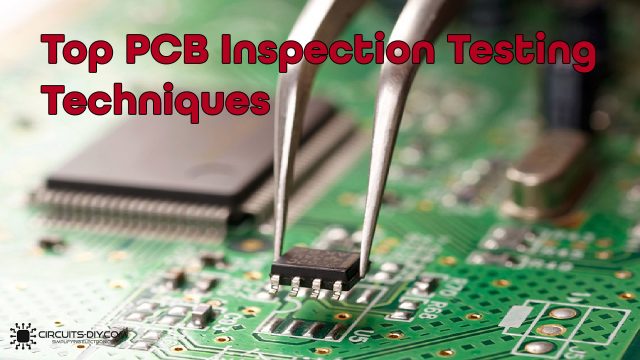 Top PCB Inspection Testing Techniques Used in Fab Houses
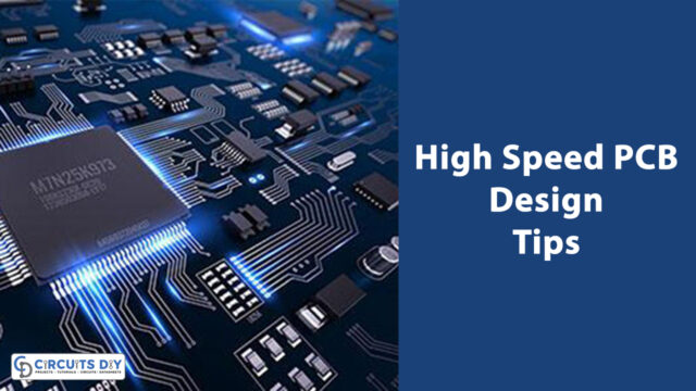 High Speed Printed Circuit Board Design Tips
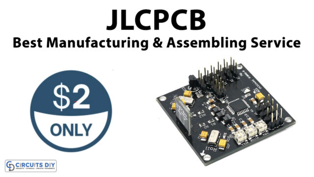 JLCPCB: An Affective Way of Manufacturing and Assembling your PCB


