CD4098 dual monostable multivibrator provides stable retriggerable/resettable one shot operation for any fixed voltage timing application. An external resistor (RX) and an external capacitor (CX) control the timing of the circuit. Adjustment of RX and CX provides a wide range of output pulse widths from the Q and Q terminals. The time delay from trigger input to output transition (trigger propagation delay) and the time delay from reset input to output transition (reset propagation delay) are independent of RX and CX. Leading edge triggering (+TR) and trailing edge triggering (-TR) inputs are provided for triggering from either edge of an input pulse.
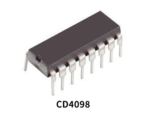
Monostable Multivibrator
A monostable multivibrator (MMV), often called a one-shot multivibrator, is a pulse generator circuit in which the duration of the pulse is determined by the R-C network, connected externally to the 555 timers. in a monostable multivibrator, a single state of the output is stable while the other is in a quasi-stable/unstable state. For auto-triggering of output from a quasi-stable state to a stable state, energy is stored by an externally connected capacitor to a reference level.
CD4098 Key Features
- High Voltage Type (20V Rating)
- Retriggerable/Resettable Capability
- Trigger and Reset Propagation Delays Independent of RX, CX
- Triggering from Leading or Trailing Edge
- Q and Q Buffered Outputs Available
- Separate Resets
- Wide Range of Output Pulse Widths
- 100% Tested for Quiescent Current at 20V
- 5V, 10V and 15V Parametric Ratings
- Standardized Symmetrical Output Characteristics
- Maximum Input Current of 1µA at 18V Over Full Package Temperature Range; 100nA at 18V and +25oC
CD4098 Pinout
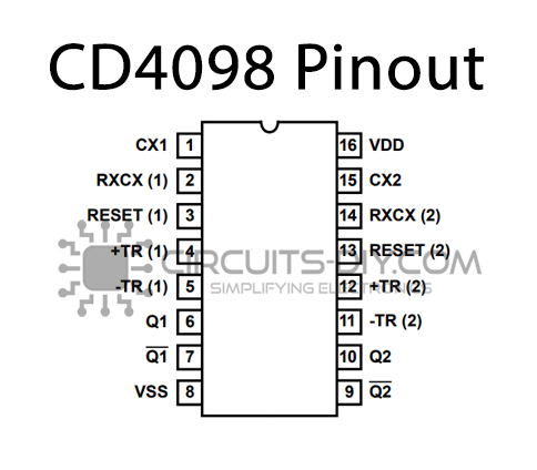
| Pin No | Pin Name | Description |
|---|---|---|
| 1 | CX1 | capacitor 1 of shift register 1 |
| 2 | RXCX (1) | resistor and capacitor of shift register 1 |
| 3 | RESET (1) | reset pin of shift register 1 |
| 4 | +TR (1) | positive trigger pin of shift register 1 |
| 5 | -TR (1) | negative trigger pin of shift register 1 |
| 6 | Q1 | output of shift register 1 |
| 7 | Q1′ | invert output of shift register 1 |
| 8 | VSS | source supply |
| 9 | Q2′ | invert output of shift register 2 |
| 10 | Q2 | output of shift register 2 |
| 11 | -TR (2) | negative trigger pin of shift register 2 |
| 12 | +TR (2) | positive trigger pin of shift register 2 |
| 13 | RESET (2) | reset pin of shift register 2 |
| 14 | RXCX (2) | resistor and capacitor of shift register 2 |
| 15 | CX2 | capacitor 2 of shift register 2 |
| 16 | VDD | Drain supply |
Application
- Pulse Delay and Timing
- Pulse Shaping
- Astable Multivibrator
CD4098 Datasheet
You can download the datasheet for CD4098 CMOS/MOS Dual Monostable Multivibrator from the link given below:
See Also: CD4541 Oscillator Programmable Timer – Datasheet | CD4503 Tri-state Hex Buffer – Datasheet | CD4543 BCD to 7-Segment Decoder – Datasheet


