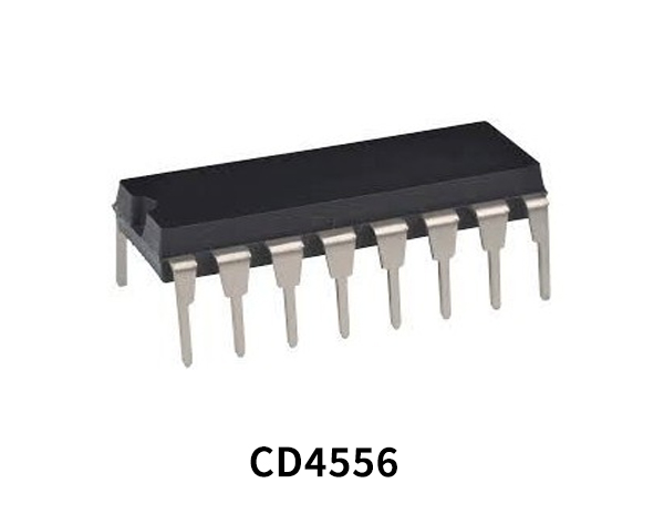
CD4556 is a part of the CD4000 IC series. CD4556 are dual one-of-four decoders/demultiplexers. Each decoder has two select inputs (A and B), an Enable input (E), and four mutually exclusive outputs. The IC is available in 16-lead hermetic dual-in-line ceramic packages. The CD4556 offers a wide array of features such as ESD protection, thermal overload protection, and a wide array of workable voltages. The IC is very simple to use and is easily interfaceable with CMOS, NMOS, and TTL
What is a Decoder?
A decoder/demultiplexer is a combinational logic circuit & an integral part of todays consumer scale electronics. It is designed to switch one common input line to one of several separate output lines. So, A demultiplexer converts a serial data signal at the input to a parallel data at its output lines.
CD4556 Key Features
- High Voltage Type (20V Rating)
- CD4555BMS: Outputs High on Select
- CD4556BMS: Outputs Low on Select
- Expandable with Multiple Packages
- 100% Tested for Quiescent Current at 20V
- Standardized, Symmetrical Output Characteristics
- Maximum Input Current of 1µA at 18V Over Full Package Temperature Range; 100nA at 18V and +25oC
- Noise Margin (Over Full Package/Temperature Range)
- 1V at VDD = 5V
- 2V at VDD = 10V
- 2.5V at VDD = 15V
- 5V, 10V and 15V Parametric Ratings
CD4556 Pinout

| Pin No | Pin Name | Description |
|---|---|---|
| 1 | E’ | invert Enable pin of decoder 1 |
| 2 | A | input pin A of decoder 1 |
| 3 | B | input pin B of decoder 1 |
| 4 | Q0A’ | invert output pin 0 0f decoder A |
| 5 | Q1A’ | invert output pin 1 0f decoder A |
| 6 | Q2A’ | invert output pin 2 0f decoder A |
| 7 | Q3A’ | invert output pin 3 0f decoder A |
| 8 | VSS | source supply |
| 9 | Q3B’ | invert output pin 3 0f decoder B |
| 10 | Q2B’ | invert output pin 2 0f decoder B |
| 11 | Q1B’ | invert output pin 1 0f decoder B |
| 12 | Q0B’ | invert output pin 0 0f decoder B |
| 13 | B | input pin B of decoder 2 |
| 14 | A | input pin A of decoder 2 |
| 15 | E’ | invert enable pin of decoder 2 |
| 16 | VDD | drain supply |
Application
- Decoding
- Code Conversion
- Demultiplexing (Using Enable Input as a Data Input
- Memory Chip-Enable Selection
- Function Selection
CD4556 Datasheet
You can download the datasheet for CD4556 Dual Binary 1 of 4 Decoder from the link given below:
See Also: 74LS398 Quadruple 2-Port Register IC | Datasheet | 74F569/74LS569 4-Bit Bi-directional Counter IC With 3-State Output | 74LS795 8-Bit Tri-State Octal Buffer IC | Datasheet

3 thoughts on “CD4556 Dual Binary 1 of 4 Decoder Inverter – Datasheet”
Comments are closed.