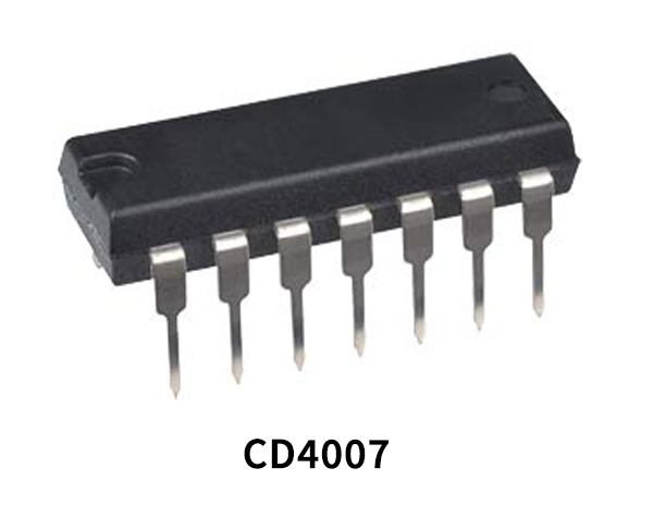
The CD4007M/CD4007C consists of three complementary pairs of N- and P-channel enhancement mode MOS transistors suitable for series/shunt applications. The IC has a wide range of working conditions and directly interfaces with CMOS, NMOS, and TTL devices. The IC offers a wide variety of applications such as low thermal dissipation and high noise immunity. For proper operation, the voltages at all pins must be constrained to be between VSS at 0.3V and VDD at 0.3V at all times. All inputs have static protection by using clamping diodes at VD and VSS.
What is an Inverter?
An inverter configuration inverts the input digital signal. An inverter always has high or logic level 1 output when its input is low or at logic level 0, and a low or logic level 0 output when input is high or at logic level 1.
CD4007 Key Features
- Wide supply voltage range: 3.0V to 15V
- High noise immunity: 0.45 VCC (typ.)
- 100% tested for quiescent current at 20V
- Standardized symmetrical output characteristics
CD4007 pinout

| Pin No | Pin Name | Description |
|---|---|---|
| 1 | 2Dp | Drain of p Channel 2 |
| 2 | 2Sp | Source of p Channel 2 |
| 3 | 2A | Input Channel 2 |
| 4 | 2Sn | Source of n Channel 2 |
| 5 | 2Dn | Drain of n Channel 2 |
| 6 | 1A | Input Channel 1 |
| 7 | VSS | Source Supply |
| 8 | 1Dn | Drain of n Channel 1 |
| 9 | 3Sn | Source of n Channel 3 |
| 10 | 3A | Input Channel 3 |
| 11 | 3Sp | Source of p Channel 3 |
| 12 | 3Y | output |
| 13 | 1Dp | Drain of p Channel 1 |
| 14 | VDD | Drain Supply |
Application
- Sharpers
- Inverters
- Threshold detectors
- Linear amplifiers
- Crystal oscillators
CD4007 Datasheet
You can download the datasheet for CD4007 Dual Complementary Pair with Inverter IC from the link given below:
See Also: CD4556 Dual Binary 1 of 4 Decoder Inverter – Datasheet | CD4521 24-Stage Frequency Divider – Datasheet | CD4538 Dual Precision Monostable Multivibrator – Datasheet