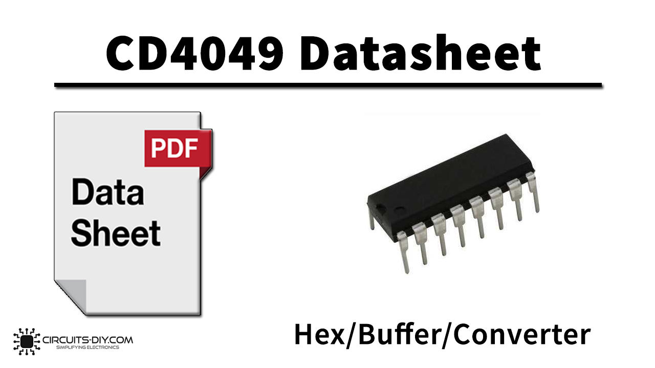
CD4049 is a part of the CD4000 IC series. The CD4049 hex buffers are made by using monolithic complementary MOS (CMOS) technology, integrated with N- and P-channel enhancement mode transistors. These devices are intended for use as hex buffers, CMOS to DTL/ TTL converters, or as CMOS current drivers, and at VDD = 5.0V, they can drive directly two DTL/TTL loads over the full operating temperature range. The IC always comes in a 16 – pin hermetically sealed dual in line IC package. CD4049

Buffer Converter
A buffer is a basic logic gate that passes its input, unchanged, to its output. Its behavior is the opposite of a NOT gate. The main purpose of a buffer is to regenerate the input, usually using a strong high and a strong low. A buffer has one input and one output; its output is always equal to its input. Buffers are also used to increase the propagation delay of circuits by driving the large capacitive loads.
Inverter
A Hex inverter is a digital logic gate that inverts the input digital signal. The output of a hex inverter is always high when the input signal is low. Similarly, a hex inverter always yields a low output when the input signal is high.
CD4049 Key Features
- Wide supply voltage range: 3.0V to 15V
- Direct drive to 2 TTL loads at 5.0V over full temperature range
- High source and sink current capability
- Special input protection permits input voltages greater than VDD
CD4049 Pinout

| Pin No | Pin Name | Description |
|---|---|---|
| 1 | VDD | Drain supply |
| 2 | G=A’ | complement output of inverter A |
| 3 | A | input of inverter A |
| 4 | H=B’ | complement output of inverter B |
| 5 | B | input of inverter B |
| 6 | I=C’ | complement output of inverter C |
| 7 | C | input of inverter C |
| 8 | VSS | source supply |
| 9 | D | input of inverter D |
| 10 | J=D’ | complement output of inverter D |
| 11 | E | input of inverter E |
| 12 | K=E’ | complement output of inverter E |
| 13 | NC | No connection |
| 14 | F | input of inverter F |
| 15 | L=F’ | complement output of inverter F |
| 16 | NC | No connection |
Application
- In CMOS hex inverter/buffer
- CMOS to DTL/TTL hex converter
- As CMOS current “sink” or “source” driver
- CMOS HIGH-to-LOW logic level converter
CD4049 Datasheet
You can download the datasheet for CD4049 Hex/Buffer/Converter IC from the link given below:
See Also: CD40110 Decade Up/Down Counter – Datasheet | CD4585 4-bit Comparator – Datasheet | CD4543 BCD to 7-Segment Decoder – Datasheet

