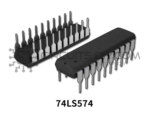
The 74LS574 is a part of the 74XXYY IC series. 74LS574 is an 8-bit, edge triggered register coupled to eight 3-State output buffers. The two sections of the IC are controlled independently by the clock (CP) and Output Enable (OE) control gates. The register is fully edge-triggered. The state of each D input, one setup time before the Low-to-High clock transition is transferred to the corresponding flip-flop’s Q output. The 3-State output buffers are designed to drive heavily loaded 3-State buses, MOS memories, or MOS microprocessors. The active Low Output Enable (OE) controls all eight 3-State buffers independently of the latch operation. When OE is Low, the latched or transparent data appears at the outputs. When OE is High, the outputs are in high impedance “off” state, which means they will neither drive nor load the bus.
What is a D-Type Flip-Flop?
A D-type Latch/flip-flop is best described as a clocked latch, that has two stable states. A D-type latch operates with a delay in input by one clock cycle. Thus, by cascading many D-type flip-flops delay circuits can be created, which are used in many applications such as in digital television systems. A D-type flip-flop is also known as a D flip-flop or a delay flip-flop.
74LS574 Pinout
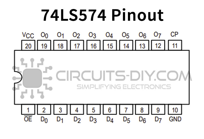
74LS574 Pin Configuration
| Pin No | Pin Name | Description |
|---|---|---|
| 1 | OE’ | Active Low 3-State Output Enable Input |
| 2 | D0 | Data Input Pin D0 |
| 3 | D1 | Data Input Pin D1 |
| 4 | D2 | Data Input Pin D2 |
| 5 | D3 | Data Input Pin D3 |
| 6 | D4 | Data Input Pin D4 |
| 7 | D5 | Data Input Pin D5 |
| 8 | D6 | Data Input Pin D6 |
| 9 | D7 | Data Input Pin D7 |
| 10 | GND | Ground Pin |
| 11 | CP’ | Clock Pulse Input (Active Low) |
| 12 | O7 | 3-State Output O7 |
| 13 | O6 | 3-State Output O6 |
| 14 | O5 | 3-State Output O5 |
| 15 | O4 | 3-State Output O4 |
| 16 | O3 | 3-State Output O3 |
| 17 | O2 | 3-State Output O2 |
| 18 | O1 | 3-State Output O1 |
| 19 | O0 | 3-State Output O0 |
| 20 | Vcc | Chip Supply Voltage |
74LS574 Features & Specifications
- Channels (#): 8
- Technology Family: LS
- VCC (Min) (V): 4.5
- VCC (Max) (V): 5.5
- Input type: Bipolar
- Output type: 3-State
- Clock Frequency (Max) (MHz): 100
- IOL (Max) (mA): 24
- IOH (Max) (mA): -3
- ICC (Max) (uA): 86000
- Propagation speed: (tpd 5-10ns)
- Edge-Triggered D-Type Inputs
- Buffered Positive Edge-Triggered Clock
- Inputs and Outputs on the opposite side of the package allow easy interface to Microprocessors
- Useful as an Input or Output port for Microprocessors
- 3-State Outputs for Bus interfacing
- Common Output Enable
- 3-State Outputs glitch-free during power-up and power-down
- ESD Protection > 4000 Volts
Applications
- Serves as a digital building block for a wide variety of temporary data storage & processing devices such as SRAMs & DRAMs etc.
- Also Useful as Input or Output Port for Microprocessors
You can download this datasheet for 74LS574 Octal Edge Triggered D-Type Flip-Flop IC from the link given below:
See Also: 74LS122 Retriggerable Monostable Multivibrator IC – Datasheet | 74LS93 4-Bit Binary/Decade Counter IC – Datasheet | 74LS86 Quad 2-Input Exclusive OR (XOR) Gate IC- Datasheet


1 thought on “74LS574 Octal Edge Triggered D-Type Flip-Flop IC With Tri-State Outputs”
Comments are closed.