74LS70 belongs to the 74XXYY IC series. The 74LS70 IC has a wide range of working voltage, a wide range of working conditions, and directly interfaces with CMOS, NMOS, and TTL. The output of the IC always comes in TTL which makes it easy to work with other TTL devices and microcontrollers. The IC offers a wide array of features such as variable operating voltages & thermal protection.

What Is a J-K Flip-Flop?
The JK Flip Flop is basically a gated RS flip flop with the addition of the clock input circuitry. When both the inputs S and R are equal to logic “1”, the invalid condition takes place. Thus to prevent this invalid condition, a clock circuit is introduced. The JK Flip Flop has four possible input combinations because of the addition of the clocked input. The four inputs are “logic 1”, ‘logic 0”. “No change’ and “Toggle”.
74LS70 Key Features & Specifications
- Technology Family: LS
- VCC (Min): 4.5V
- VCC (Max): 5.5V
- Max Propagation delay 35ns
- IOL (Max): -0.4mA
- IOH (Max): 8mA
- Rating: Military
- TTL outputs
- Low power consumption
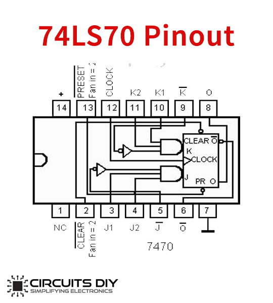
74LS70 Pinout
| Pin Name | Pin No. | Description |
|---|---|---|
| NC | 1 | Not Used |
| CLR/fan in = 2 | 2 | Clear Active low |
| J1 | 3 | J Flip-Flop Input pin 1 |
| J2 | 4 | J Flip-Flop Input pin 2 |
| J | 5 | Active low J input |
| O | 6 | Active low output pin |
| GND | 7 | Ground pin |
| O | 8 | Outpin pin active high |
| K | 9 | Active low K input |
| K1 | 10 | K Flip-Flop Input pin 1 |
| K2 | 11 | K Flip-Flop Input pin 2 |
| CLK | 12 | Clock Input pin |
| PRESET/fan in = 2 | 13 | Preset pin Active low |
| VCC | 14 | Chip Supply Voltage |
Applications
The 74LS70 IC has a number applications, a few are listed below:
- They are used in digital clocks, electronic meters, and other electronic devices that display numerical information.
74LS70 Datasheet
You can download the 74LS70 J-K Positive Edge Triggered Flip-Flop IC Datasheet from the link given below:
See Also: 74LS20 Dual 4 – Input NAND IC | 74LS02 Quad Two Input NOR Gate| 7407 Hex Buffer IC