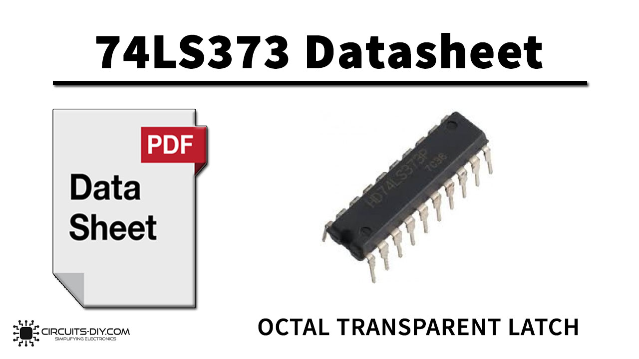
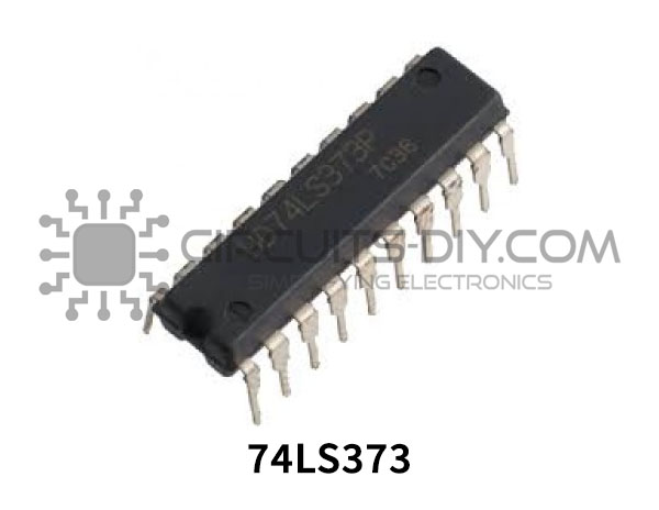
The 74LS373 IC consists of eight D-Type latches/Flip-Flops with 3-state outputs for bus organized system applications. The high-impedance state and increased high-logic level drive provide these registers with the capability of being connected directly to and driving the bus lines in a bus-organized system without the need for interface or pull-up components. The eight latches of the 74LS373 are transparent D-type latches, meaning that while the enable (C or CLK) input is high, the Q outputs follow the data (D) inputs. When C or CLK is low, the output is latched at the level of the data that was set up. 74LS373 IC has a wide range of working voltage, a wide range of working conditions, and directly interfaces with CMOS, NMOS, and TTL. The IC 74LS373 is smaller in size and it has a much faster speed which makes it reliable in every kind of device.
What is a D-Type Latch/Flip-Flop?
A D-type Latch/flip-flop is a clocked latch which has two stable states. A D-type latch operates with a delay in input by one clock cycle. Thus, by cascading many D-type flip-flops delay circuits can be created, which are used in many applications such as in digital television systems. A D-type flip-flop is also known as a D flip-flop or a delay flip-flop.
74LS373 Pinout

74LS373 Pin Configuration
| Pin No | Pin Name | Description |
|---|---|---|
| 1 | OE’ | Active Low Output Enable Pin |
| 2 | O0 | Output Pin 0 |
| 3 | D0 | Data Input Pin 0 |
| 4 | D1 | Data Input Pin 1 |
| 5 | O1 | Output Pin 1 |
| 6 | O2 | Output Pin 2 |
| 7 | D2 | Data Input Pin 2 |
| 8 | D3 | Data Input Pin 3 |
| 9 | O3 | Output Pin 3 |
| 10 | GND | Ground Pin |
| 11 | LE | Latch Enable Input |
| 12 | O4 | Output Pin 4 |
| 13 | D4 | Data Input Pin 4 |
| 14 | D5 | Data Input Pin 5 |
| 15 | O5 | Output Pin 5 |
| 16 | O6 | Output Pin 6 |
| 17 | D6 | Data Input Pin 6 |
| 18 | D7 | Data Input Pin 7 |
| 19 | O7 | Output Pin 7 |
| 20 | Vcc | Chip Supply Voltage |
74LS373 Features & Specifications
- Channels (#): 8
- Technology Family: LS
- VCC (Min): 4.75V
- VCC (Max): 5.25V
- Input type: Bipolar
- Output type: 3-State
- Clock Frequency (Max): 35MHz
- IOL (Max): 24mA
- IOH (Max): -2.6mA
- ICC (Max): 40000uA
- Propagation speed: (tpd 10-50ns)
- 3-State Outputs for Driving Highly Capacitive or Low Impedance Loads
- Choice of 8 D-type Flip-Flops in a Single Package
- Full Parallel Access for Loading
- Buffered Control Inputs
- Standard TTL Switching Voltages
Applications
- They are particularly useful for implementing buffer registers, I/O ports, bidirectional bus drivers, and working registers in modern computing systems.
You can download this datasheet for 74LS373 from the link given below:
See Also: 74LS08 Quadruple Two Input AND Gate – Datasheet | 74LS164 8-Bit Shift Register IC With Parallel Outputs – Datasheet | 74LS151 8 To 1 Line Selector Multiplexer IC – Datasheet

