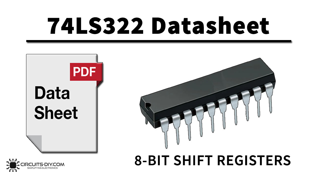
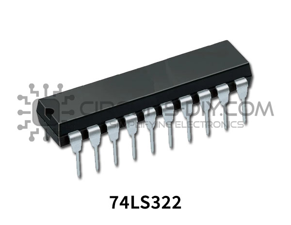
The 74LS322 is an 8-bit shift register with provision for either serial or parallel loading and with 3-state parallel outputs plus a bi-state serial output. Four synchronous modes of operation are possible: hold (store), shift right with serial entry, shift right with sign extend, and parallel load. An asynchronous Master Reset (MR) input overrides clocked operation and clears the register.
Functional Description
The 74LS322 IC contains eight D-type edge-triggered flip-flops and the interstage gating required to perform the right shift and the interstage gating necessary for hold and synchronous parallel load operations. A LOW signal on RE enables shifting or parallel loading, while a HIGH signal enables the hold mode. A HIGH signal on S/P enables shift right, while a LOW signal disables the 3-state output buffers and enables parallel loading. In the shift right mode, a HIGH signal on SE enables serial entry from either D0 or D1, as determined by the S input. A LOW signal on SE enables shift right but Q7 reloads its contents, thus performing the sign extend function. A HIGH signal on OE disables the 3-state output buffers regardless of the other control inputs. In this condition, the shifting and loading operations can still be performed
What is a Shift Register?
Storage/Shift registers are digital memory circuitry found in various types of equipment & tools such as calculators, computers, and data processing systems. With a shift register, data or bits are entered into the system in a serial or parallel manner. data entry is done from one direction, and as more data is added, it shifts positions until the data gets to the output end. The two ends are referred to as the left and right end. Movement of data can be from left to right, from right to left, or in both directions to make a bidirectional register.
74LS322 Key Features & Specifications
- Bits (#): 8
- Technology Family: LS
- VCC (Min) (V): 4.75
- VCC (Max) (V): 5.25
- Input type: TTL
- Output type: TTL
- IOL (Max) (mA): 24
- IOH (Max) (mA): -2.6
- Multiplexed Input/Outputs for Data Hold, Shift Right, Shift Left, and Load Data
- Multiplexed Inputs/Outputs to provide Improved Bit Density
- Sign Extend Function
- Direct Overriding Clear
- 3-State Outputs Drive Bus Lines Directly
74LS322 Pinout
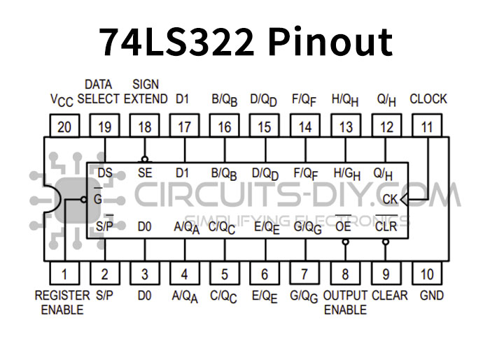
| Pin No. | Pin Name | Description |
|---|---|---|
| 1 | G’ | Active low Register Enable input |
| 2 | S/P’ | Serial (HIGH)/Parallel (LOW) Mode Control Input |
| 3 | D0 | Serial Data Input Pin D0 |
| 4 | A/Qa | Multiplexed Parallel I/O Pin A |
| 5 | C/Qc | Multiplexed Parallel I/O Pin C |
| 6 | E/Qe | Multiplexed Parallel I/O Pin E |
| 7 | G/Qg | Multiplexed Parallel I/O Pin G |
| 8 | OE’ | Active Low Output Enable Pin |
| 9 | CLR’/MR’ | Active Low Master Reset/Clear Input |
| 10 | GND | Ground Pin |
| 11 | CLK | Clock Pulse Input |
| 12 | Q/H | Bi-State Serial Output |
| 13 | H/Qh | Multiplexed Parallel I/O Pin H |
| 14 | F/Qf | Multiplexed Parallel I/O Pin F |
| 15 | D/Qd | Multiplexed Parallel I/O Pin D |
| 16 | B/Qb | Multiplexed Parallel I/O Pin B |
| 17 | D1 | Serial Data Input Pin D1 |
| 18 | SE’ | Active Low Sign Extend Input |
| 19 | DS | Serial Data Select Input |
| 20 | Vcc | Chip Supply Voltage |
Applications
The 74LS322 has a wide variety of applications. A few of them, are listed down below:
- Usually used in designing sequence generation circuits.
74LS322 Datasheet
You can download the datasheet for 74LS322 8-Bit Shift Registers IC With Sign Extend from the link provided below:
See Also: 74LS153 Dual 4 To 1 Line Multiplexer IC – Datasheet | 74LS139 Dual 1-Of-4 Decoder/Demultiplexer IC – Datasheet | 74LS157 Quad 2 To 1 Line Multiplexer IC – Datasheet


