
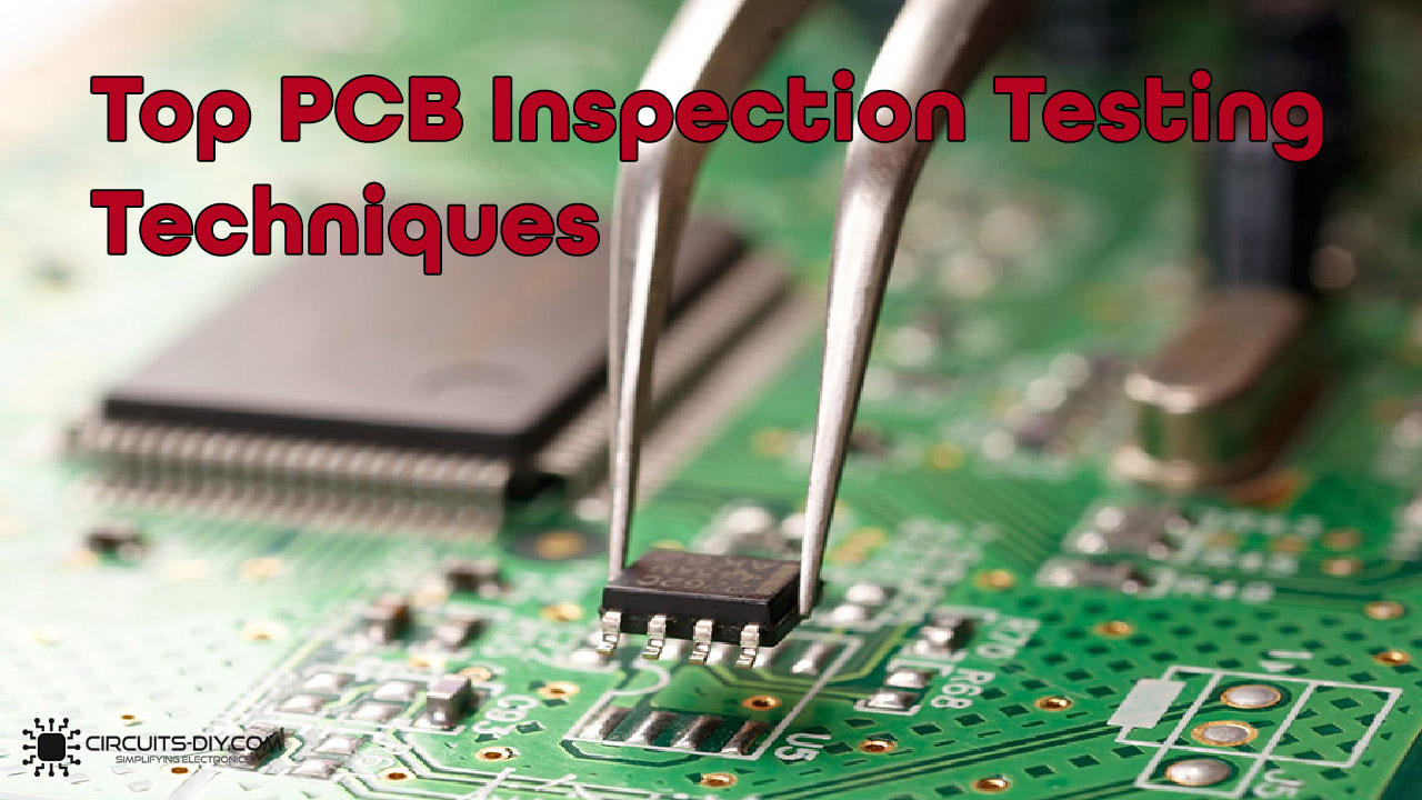
PCB Inspection/Testing techniques are an important part of PCB manufacturing before production. These evaluative tests are essential in determining the quality of your final product. Even after following proper design and manufacturing processes, there is always a risk of defects, bugs, human errors at the prototype stages. Identifying and addressing these issues before the final product is critical in ensuring the performance, functionality, and reliability of the products. A great number of popular Electronic contract manufacturers (ECMs) offer a wide range of QA tests in order to ensure the quality of your PCB boards. So, in today’s article, we are going to go over the top PCB Inspection/Testing Techniques Used in PCB Fab Houses.
Top PCB Inspection/Testing Techniques Used In PCB Manufacturing
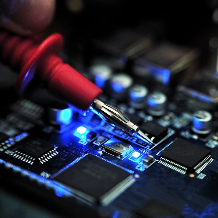
1) In-Circuit Testing
In-Circuit testing is a fully automated test, which detects defects in an assembly of PCBs through ‘Schematic verification’. ICT works in two parts, namely the Power-off & Power-on test. ICT identifies a large number of defects in the assembly; which includes, but is not limit to Component markings, Presence/absence of passive components, etc.
2) Time Domain Reflectometry Test (TDR Test)
Time Domain Reflectometry (TDR); in literal sense, allows the design engineer to determine the characteristic impedance of the PCB board or card in a test. TDR test also helps in determining whether if the differential traces present on the PCB board are a complete match for good signal integrity or not.

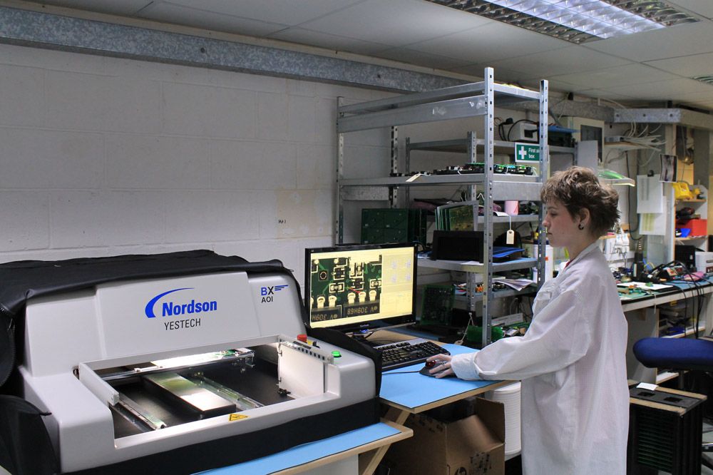
3) Automated Optical Inspection (AOI) Test
AOI tests use a single 2D or two 3D camera’s visual input to monitor PCBs for defects. This method is only useful on PCBs where the points to test are optically visible. It is performed to check solder quality and verify pad and trace connections. AOI is also very useful for the early detection of assembly issues.
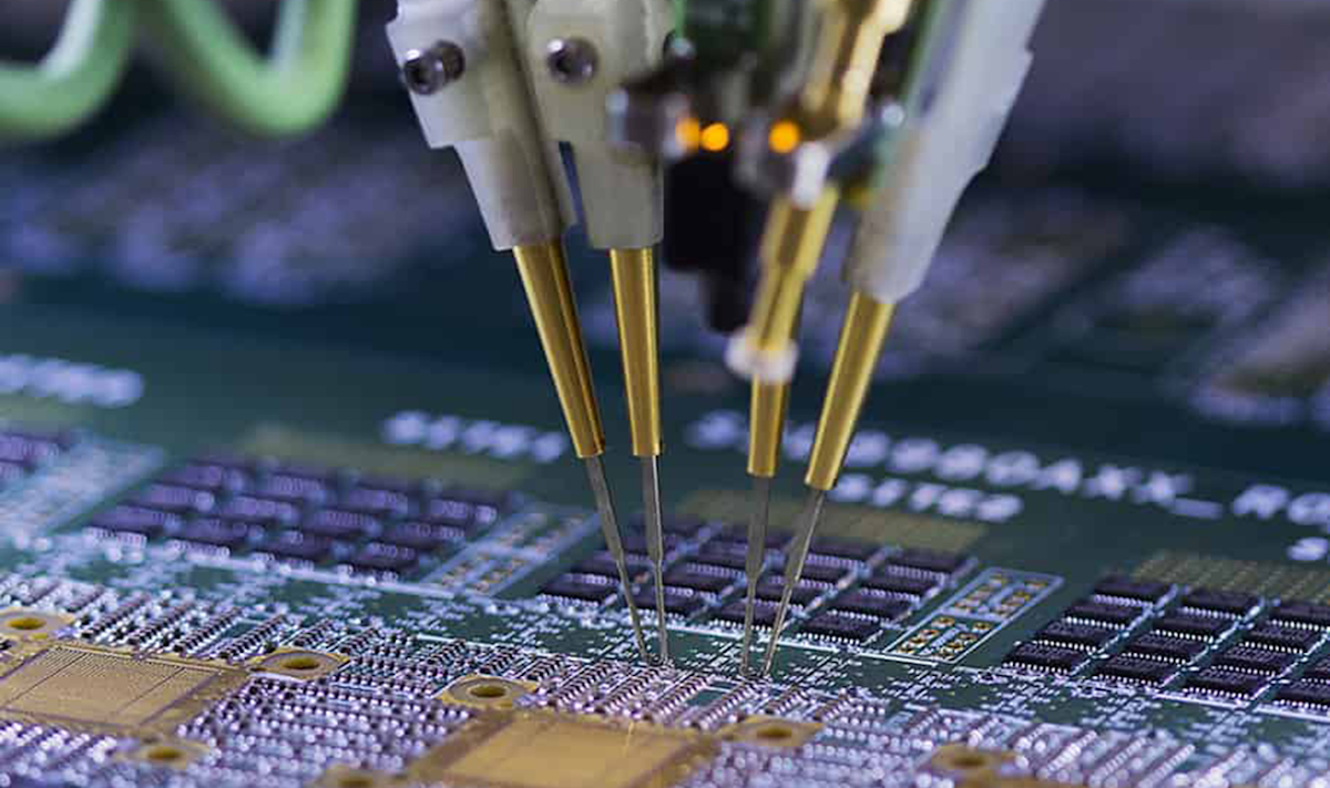
4) Flying Probe Test
The Flying Probe test is a tested & true option that is inexpensive than In-circuit testing. The technique uses an element with a smaller pitch; in order to, make contact with the test points such as the SMD pins. It can test vias & pads to detect defects of a PCB unit.
5) Resistivity Of Solvent Extract (ROSE) Test
ROSE Testing is a highly reliable test that usually serves to ensure that a PCB board does not contain any significant surface debris remaining; especially, from manufacturing processes or excess conductive material.

6) X-Ray Inspection
The X-Ray or AXI can detect elements that are usually hidden from view, such as internal traces & ball grid array packages with solder joints under the chip package. There are 2D & 3D AXI tests available in today’s PCB industry, with 3D offering a faster testing period.

7) Functional Test
Functional tests for PCBs are come usually at the end. FCT verifies a PCBs function & behavior, in various simulated field environments. Usually, the parameters of an FCT is up to the customers’ desire. Moreover, FCT also verifies whether or not a PCB is ready to run in a real time stress environment.
Related posts:
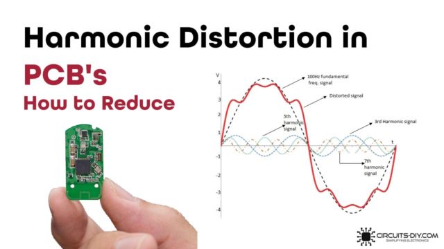 Harmonic Distortion in PCB's - How to Reduce
 Aluminum PCB Manufacturer
 6 Tips to Reduce PCB Size for Your Projects
 Reducing PCB Prototype Failure Using DRC | Guide For Beginners
 PCB Design Issues Faced In PCB Manufacturing & Their Troubleshooting
 SMT PCB Reflow Soldering Process | Everything You need to Know


