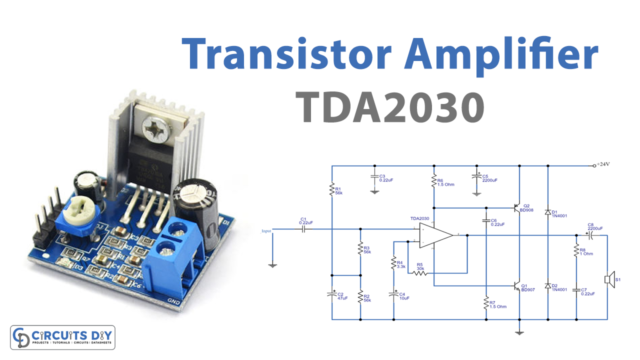

The growing demand for more compact and complicated electronic products requires PCBs with multiple layers. As such the importance of stackup has grown a lot in recent times, with the production of increasingly more complex PCBs which are composed of many layers. The first PCB prototypes were simple and can only serve as a connection base for electronic components. For their simplicity, the need to stack multiple layers was minimal.
Stackup is an important part of the PCB design and a good stack-up design is a key to reduce electromagnetic emission (EM) from electronic circuitry. Thus, improving the overall signal integrity of the circuit board. On the other hand, a poor stack-up design can lead to higher EM emission and signal losses. The job of every PCB designer is to reduce EM emission from the loops on the PCB caused due to the differential-mode noise and common-mode emission.
There are three important factors to consider when we are designing PCB stackup:
- Number of Layers
- Layer material
- Layer arrangement
Number of layers
When deciding number of layers for PCB stackup we have to consider signal (high or low speed), power, and ground layers or planes. It is highly recommended not to mix different types of signals on inner layers.
The number of layers in PCB also depends on pin density and signal layers. A pin density of 1.0 will necessitate 2 signal layers. The number of necessary layers goes up as the pin density drops for example a pin density of 0.2 means you will need PCBs with at least 10 layers.
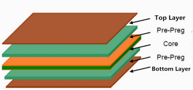
Layer material
When deciding PCB layer material any engineer should consider thermal, mechanical and electrical, properties involved in the process. This should be established in conjunction with determining thicknesses for prepreg and cores. Each circuit board material has different standard thicknesses and properties.

Layer arrangement
Some of the rules to determine how layers should be arranged are given below:
- Always place signal layers next to internal power layers for tight coupling.
- Spacing between power and ground layers should be minimal.
- Route high-speed on minimum thickness microstrips.
- Avoid having two signal layers adjacent to each other.
- Try making stack up symmetric from the top and bottom layers.