Printed circuit boards are the major part of electronic circuits. In this article, we are going to analyze different types of PCBs
Single Layer
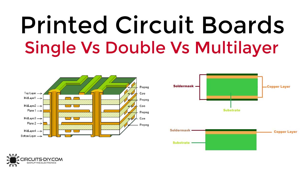
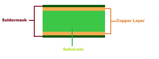
Single-layer PCBs are the printed circuit boards having a single side of conducting material. In other words, they have just one side of the substrate to design the circuit. However, they are not sufficiently promising for complex circuits. And, not effective for complicated devices

Double Layer
Double layer PCB is very identical to a single-layer PCB. However, they have two sides that have copper conductive material. That allows the tracks to cross over each other. As a result, it gives higher density to circuits without a point to point soldering. The double-layer is the most popular type of PCB that has so many applications
Multi-layer
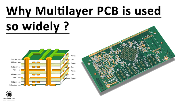
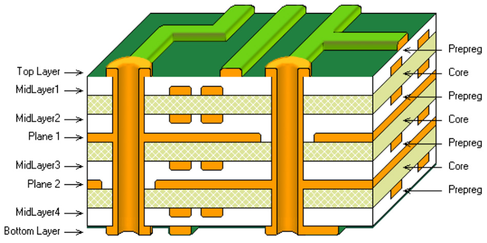
Multi-layer PCB. Multi layer are the major and most beneficial type of Printed Circuit boards. Multi-layer PCBs include three dual-size copper layers that enable a complete layer for the ground plane. We can operate thousands of components and ten thousands of vias in multilayer PCB. Greatly used multi layers have less than 10 conducting layer and have a thickness of 1.5mm.
JLCPCB is the foremost PCB prototype & manufacturing company in china, providing us with the best service we have ever experienced regarding (Quality, Price Service & Time).
Manufacturing Process of Printed Circuit Boards
Single Layer
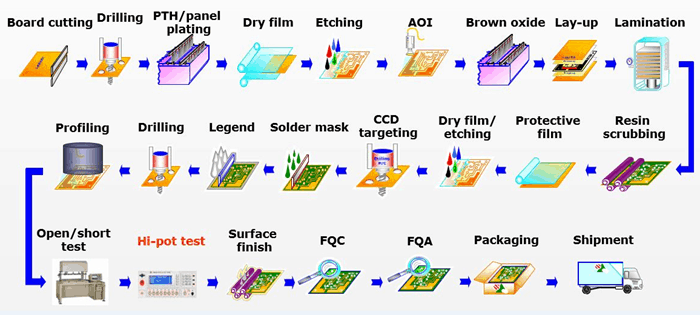
- Designing of Circuit: The first step is to design the circuit layout on the software. Once the design is made, it gets a recheck if there are any errors.
- Printing of the Design: The design then gets printed on paper. A special plotted printer is used for this purpose.
- Substrate Creation: The substrate gets created using iron the design on the thin PCB board. And, then etched away to illustrate the design from printed films. The photoreactive film makes the resist. This chemical gets harder after exposure to ultraviolet light.
- Inspection And Lamination: An optical punch device drills a pinto to keep the layers mobilized. After that, another machine inspects the board to make sure that there are no errors or flaws. The epoxy resin layer goes on the alignment compartment. Then a layer of substrate goes over this epoxy resin pursued by copper foil.
- Drilling And Plating: To press the layer, there use the mechanical press. Then, PCB goes to laminating press which applies pressure and heat to the board. After that, holes are drilled into the layer, and the remaining copper gets removed. Now, the panel is plated with a copper layer and a thin ton guard is layered on the board. The thin tin guard is used to protect the copper.
- Etching and Solder Mask: The chemical used before removes the unwanted copper and creates the connection on board. Then the solder mask. Solder mask usually involves those green colors that you on the PCB board. After that, ultra Violet light removes the solder mask.
- Silk Screening and Testing: Silk screening prints the crucial information on board. Lastly, designers perform a testing
Double and Multi-Layer
Everything remains the same except the lemination of copper. The substrate goes on every layer. Also, surface mount technology got introduced.
Applications of Printed Circuit Boards
Single Layer
- In photocopy and printer machines
- For vending machine circuits
- Solid-state devices and equipment
- In the circuit of digital cameras
- In radio circuits
- Used in digital and analog power supply
Double Layer
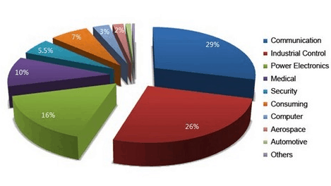
- Medical devices
- Industrial machinery
- Aerospace applications
- Lightning application
Multi Layer
- In Computer Electronics: Multilayer PCBs have highly used in computer electronics. Since computer needs high efficiency and speed. Therefore, they are highly preferable.
- Medical Appliances: Multilayer PCB is promising for medical equipment. The reason is its functionality and durability. As we have discussed earlier that it has a high durability rate.
- Telecommunication: It has various applications in telecommunication. For example, they are in GPS and satellites. Also, it has applications in signal transmission.
- Military: Highly preferable in military applications. As it has high speed and low weight. And, also it has high durability.


