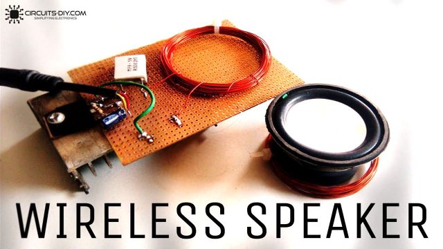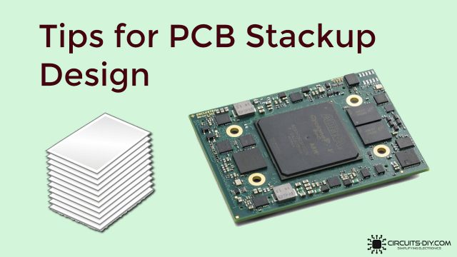
Introduction
In this modern age of big data and IoT, the demand for wireless products is enormously higher. About every other electronic device has wireless communications. Thus, it requires transmitter and receiver boards to communicate effectively over small and large areas. All the wearable and compact devices utilize wireless communication networks. Wireless communication includes Bluetooth, wi-fi, mobile networks, RF signals, etc. These kinds of communication need powerful performance and a high data rate with high frequency. Thus, in this article, we will study guidelines for the printed circuit boards that are used in wireless electronic devices and products.
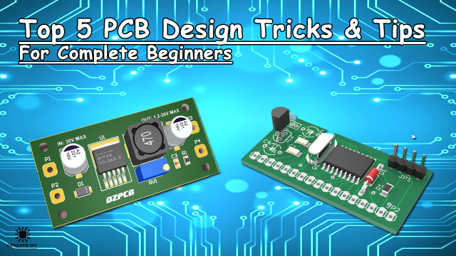
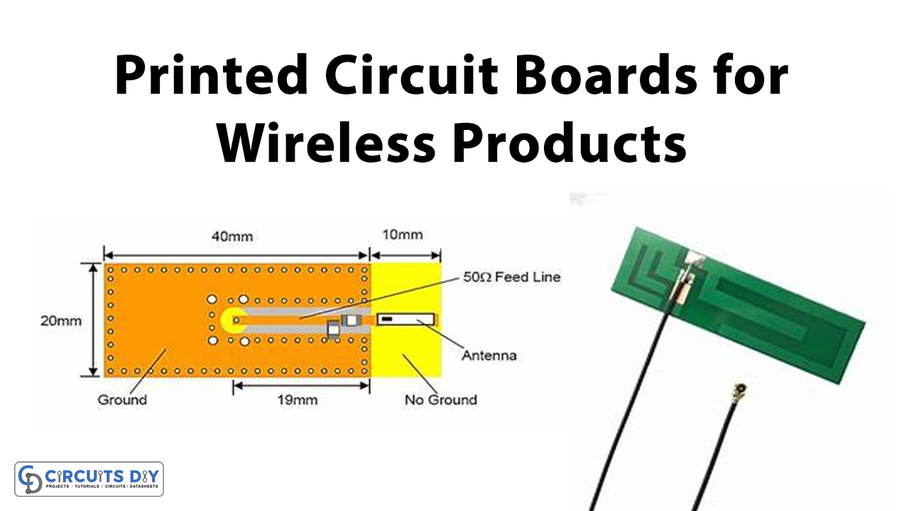
Tips for Wireless Printed Circuit Boards
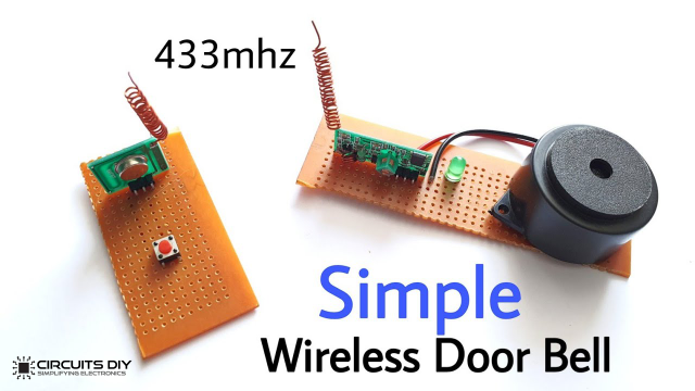
To create better-printed circuit boards for GPS, RF signals, Bluetooth devices, IR communications, etc, we have comprehended three main guidelines to make a better PCB. Those are:
- Better antenna type.
- Ground planes near antennas.
- High gain design.
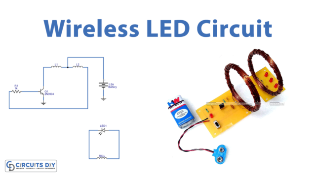
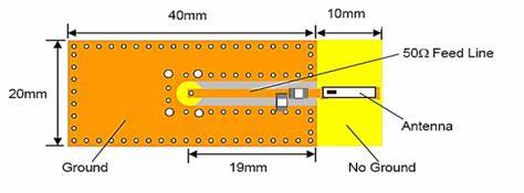
Antenna Type for Printed Circuit Boards
Different wireless connections need diverse kinds of antennas. Remember, the smaller antennas always hold higher frequencies. However, it is difficult to find external antennas for higher frequencies. In short, use the antennas according to the requirement of your device frequency. For example, RF PCB design products demand PCB antennas of about 110GHz. Consequently, antennas can easily be mounted directly on the printed circuit boards. But, the directly mounted antennas are not useful for greater bandwidths. For the greater bandwidths, antennas are placed in high-frequency packages on the printed circuit boards. But, they are very expensive. Now, to overcome the expanses, the type of antennas can be used that is connected directly to the Integrated circuits. Moreover, this kind of antenna is more efficient for high frequencies. However, doesn’t work for lower frequencies.
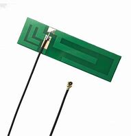
Antennas near the Ground Planes
As you already know that the main objective of the antennas is to transmit signals or receive radiated signals. In anyways, they hold signals. Since antennas carry some signals and those signals require the return path. Therefore, it is crucial to mount the antennas near the ground planes. So that, it can provide a smaller return path. Moreover, this technique also reduces the EMI problems that can arise in the circuit. In other words, whether you use traced antennas, pre-packaged antennas, or any other kind of antennas, they must have to be placed near the ground planes.
High Gain Design
To make an efficient printed circuit board, it is necessary to choose the design parameters that maximize the gain of the antennas mounted n the printed circuit boards. Because the gain of the antennas is directly proportional to the transmission of the signal, dielectric efficiency, and conduction efficiency. Thus, we cannot deny the fact that it is challenging to measure dielectric and conduction efficiencies. But, the estimation can be done by different practices. Conduction efficiency can be evaluated by the conductor in the antenna. Therefore, choosing the best kind of conductor would be a great choice for greater conduction efficiency. For greater dielectric efficiency, use good material for the manufacturing of the PCB. This can reduce dielectric losses.