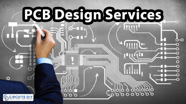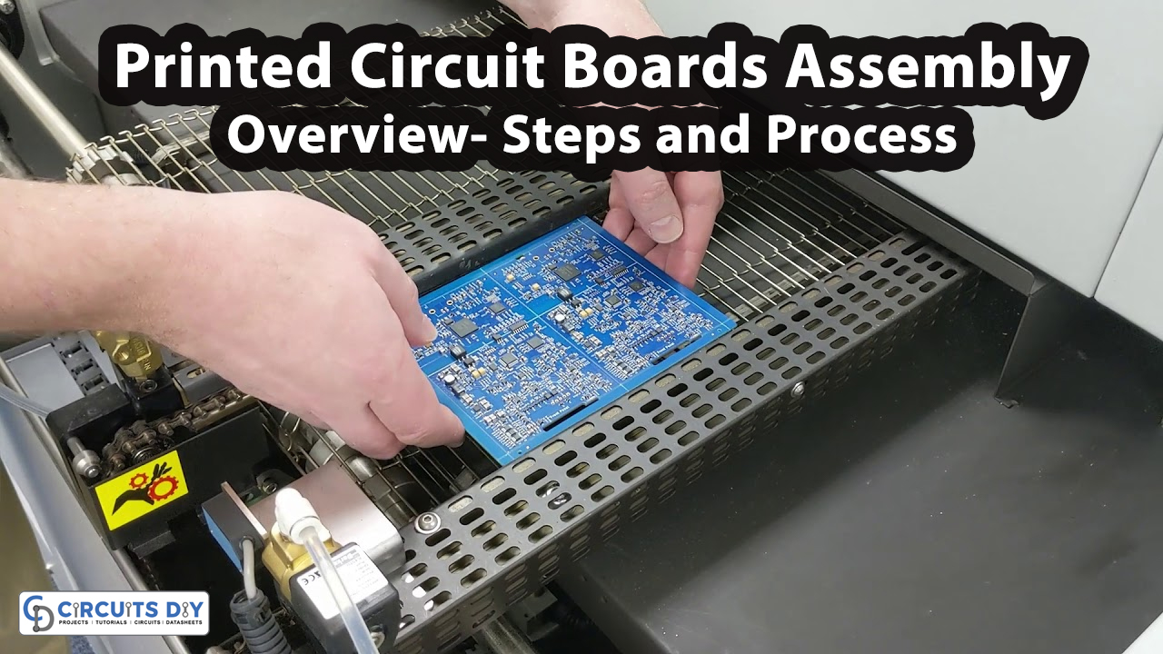
Introduction
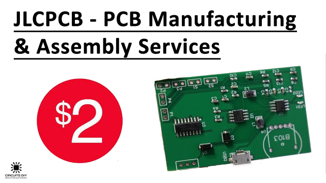
As we have already known that electronic products highly adopt printed circuit boards for their applications. Also, we acknowledge that printed circuit boards come in numerous qualities and types. However, all the types practice the same assembly process. The printed circuit board PCB assembly process ensures the better quality of the PCB. Therefore, in this article, we will overview the printed circuit board assembly.
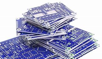
Elements Required for PCB Assembly
Before discussing the assembly process, look at the elements that one needs to require. Those elements and the components are:
- Plain printed circuit Board
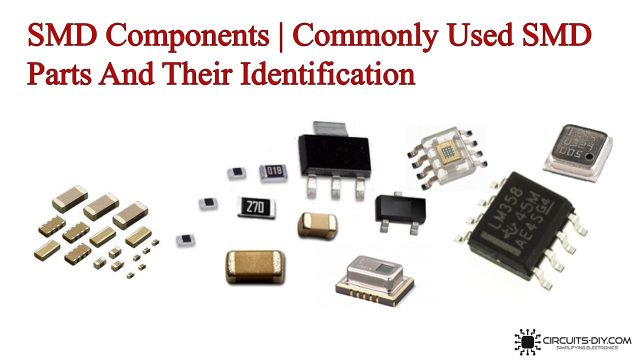
- Electronic components to build a circuit
- Soldering elements like solder paste, soldering wire, etc
- Testing and inspection equipment
Steps of Assembly of Printed Circuit boards
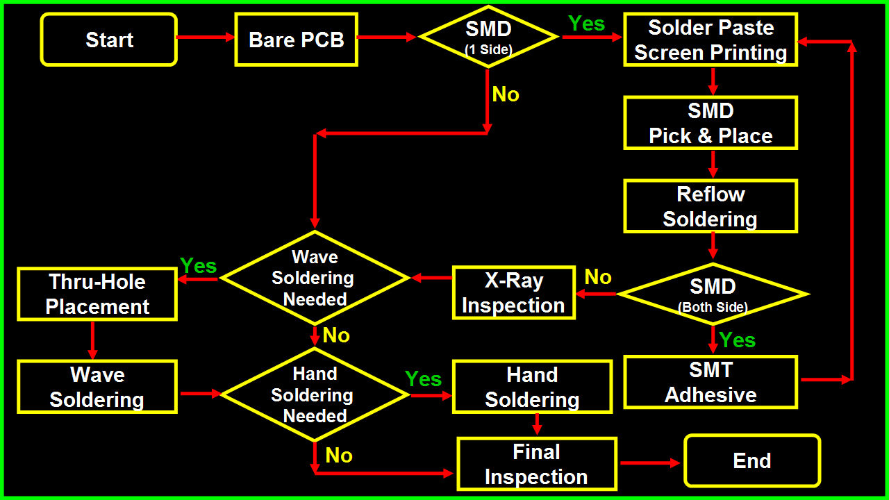
Printed circuit board assembly requires several steps. Those steps are:
- Solder paste stenciling.
- Placement of SMT components.
- Reflow soldering.
- Inspection.
- Insertion of through-hole components.
- Functional test.
1. Solder paste Stenciling
This is the very first step of the PCB assembly. This allows the application of solder paste, where the components are going to be placed. A solder paste usually is a homogeneous mixture of alloy powder and solder flux. Thus, the most common alloy powder are Sn-Pb, Sn-Cu, Sn-Ag-Cu, etc. Hence, the most common solder flux includes a thixotropic agent, a solvent, resin, and an activator. Certainly, the solder flux is the fundamental material that prevents the soldering material from oxidation and cleans the metal surfaces. Moreover, the soldering flux has greater stability for the storage of solder paste. When applying on the PCB, remember to stir it before for the proper application of the uniform viscosity
2. Placement of SMT Components
Now, after the paste has been applied, the Surface mounted components get placed. The SMD mounting doesn’t require any connector. Hence, the components are placed above the applied solder paste. But, it requires an automated machine to perform the process. However, the process can also be completed manually by using tweezers.
3. Reflow Soldering
After the solder paste has been applied and the SMD gets mounted, now the components need to be secure. And, this is possible through the process of reflow. Therefore, Board expects heat to melt the solder paste so that it makes a connection to the pads and the leads. Importantly, at first, the fewer component side that has fewer elements performs stenciling, placement, and reflow.
6. Inspection
After the reflow method, there is a time to inspect the errors and check the misalignments. Mainly there are three different methods for the inspection. The first is the manual check method through which the errors are checked manually. Then, there is an automatic optical inspection method that uses high-power cameras for inspection. Further, there is an X-ray inspection method that uses X-ray. However, it is rarely in use.
5. Insertion of Through-Hole Components
Now, is the time, to insert the through-hole components that need the connectors. Through-hole components don’t require solder paste. But, it requires soldering. And, soldering can be done through two different methods:
- Manual Method: Manually the insertion can be completed through soldering iron.
- Wave Soldering Method: It’s an automated method that allows different processes.
6. Functional Test
Finally, this is the time for a final inspection. Therefore, this final inspection is known as a functional test. Moreover, this determines the failure or the success of the PCB assembly process. Hence, necessary to perform.