In this project, we will develop a circuit for One Bit Memory Cell. The data was stored in the memory of all embedded devices. This memory consists of flip-flops that store the data in bits. These flip-flops store data. You can store one bit for each flip-flop. We’ll have 8-bit memory for eight flip-flops.
This memory is used for storing or accessing programs. Here we are talking about SR flip-flops of various kinds. There is a flip-flop in the 555 IC timer so that the timer can be set up to save one bit of data. That’s what we’ll do here. We use the timer to store only one bit of data.
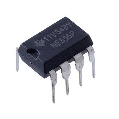
Hardware Component
The following components are required to make One Bit Memory Cell Circuit
| S.no | Component | Value | Qty |
|---|---|---|---|
| 1. | Supply voltage | +5 to +12 V | 1 |
| 2. | IC | NE555 Timer | 1 |
| 3. | Resistor | 1KΩ, 10KΩ | 1, 2 |
| 4. | Button | – | 2 |
| 5. | LED | – | 1 |
| 6. | Capacitor | 100µF | 1 |
NE555 IC Pinout
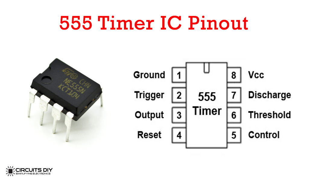
For a detailed description of pinout, dimension features, and specifications download the datasheet of 555 Timer
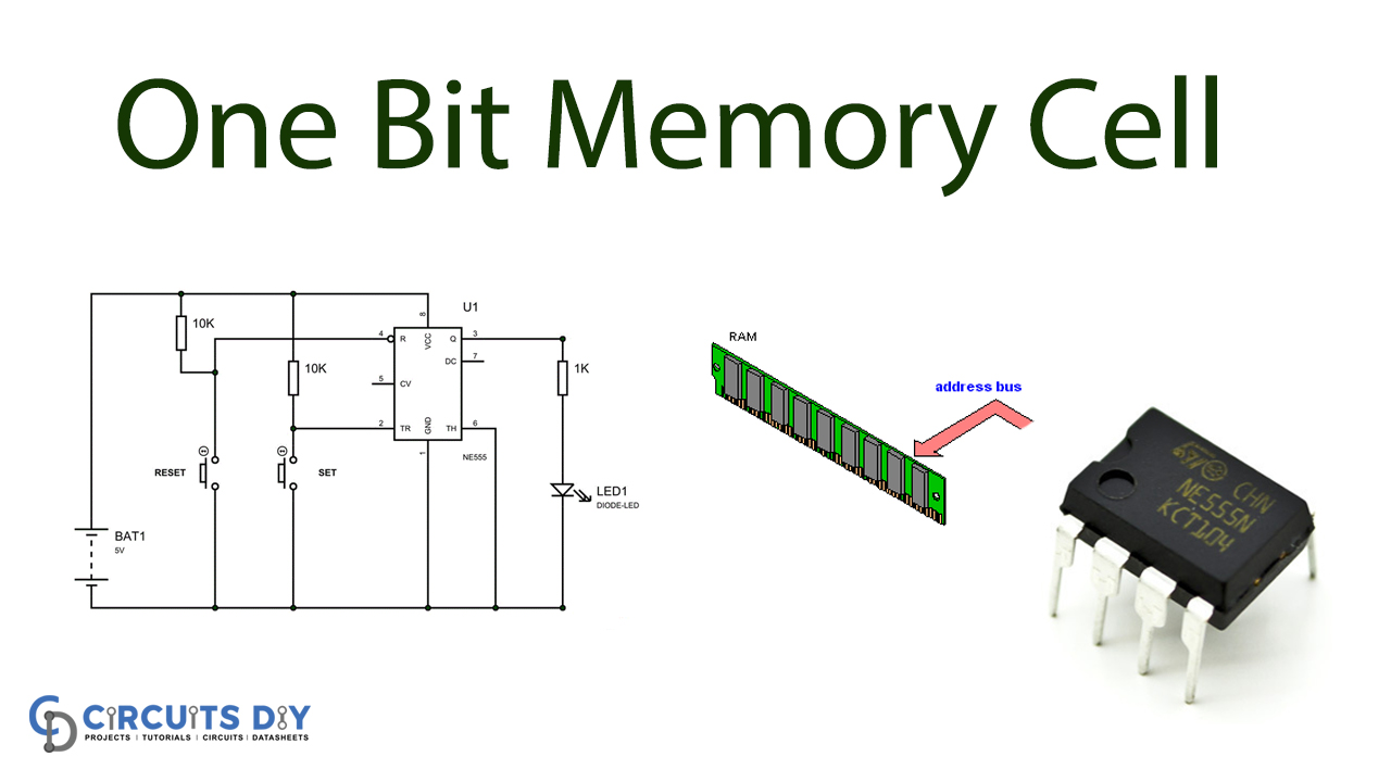
One Bit Memory Cell Circuit

Working Explanation
This figure displays the circuit diagram of a 1-bit memory-based 555 timer IC. We use the timer flip-flop here, as we mentioned previously.
Taking all the components into account now, as seen in the circuit diagram, the power is triggered. The second comparator would be low since the threshold pin is connected with the 10 K resistor’s power. The second SET pin of the flip-flop in the timer is fed with this signal.
The flip-flop receives a low signal on the flip-flop set pin, as seen below.
This positive high signal is driven to the Flip-flop setting pin, and thus a flip-flop store ONE has a high Q output such that the timer output can be high.
Applications and Uses
It enables all programs to store data and allows for the temporary storing of combination-circuit output to be used by digital devices in memory cells. Sequential circuits are called logic circuits and use memory cells.


