Contents
hide
MC3487 Quad Line Driver, Three-State features four independent driver chains which comply with EIA Standards for the Electrical Characteristics of Balanced Voltage Digital Interface Circuits. The outputs are three–state structures which are forced to a high impedance state when the appropriate output control pin reaches a logic zero condition. All input pins are PNP buffered to minimize input loading for either logic one or logic zero inputs. In addition, internal circuitry assures a high impedance output state during the transition between power up and power
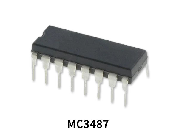
MC3487 Pinout
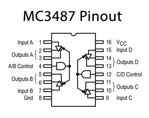
MC3487 Pin Configuration
| Pin No | Pin Name | Description |
|---|---|---|
| 1 | IN A | Input Pin A |
| 2 | OUT A1 | Output Pin A1 |
| 3 | OUT A2 | Output Pin A2 |
| 4 | A/B CNTRL | A/B Control Pin |
| 5 | OUT B1 | Output Pin B1 |
| 6 | OUT B2 | Output Pin B2 |
| 7 | IN B | Input Pin B |
| 8 | GND | Ground Pin |
| 9 | IN C | Input Pin C |
| 10 | OUT C1 | Output Pin C1 |
| 11 | OUT C2 | Output Pin C2 |
| 12 | C/D CNTRL | C/D Control Pin |
| 13 | OUT D1 | Output Pin D1 |
| 14 | OUT D2 | Output Pin D2 |
| 15 | IN D | Input Pin D |
| 16 | VCC | Collector Supply Voltage |
MC3487 Key Features
- Four Independent Driver Chains
- Three–State Outputs
- PNP High Impedance Inputs (PIA Compatible)
- Fast Propagation Times (Typical 15 ns)
- TTL Compatible
- Single 5.0 V Supply Voltage
- Output Rise and Fall Times Less Than 20 ns
- DS 3487 Provides Second So
You can download this datasheet for MC3487 Quad Line Driver, Three-State from the link given below:


