Contents
hide
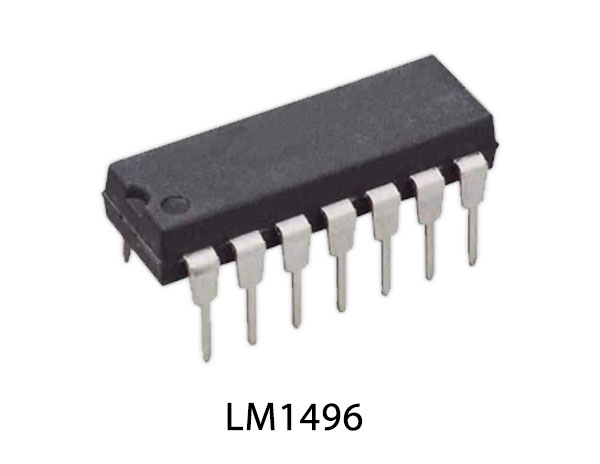
The LM1496 is doubled balanced modulator-demodulators which produces an output voltage proportional to the product of an input (signal) voltage and a switching (carrier) signal. Typical applications include suppressed carrier modulation, amplitude modulation, synchronous detection, FM or PM detection, broadband frequency doubling, and chopping. The LM1496 is specified for operation over the 0C to a70C temperature range.

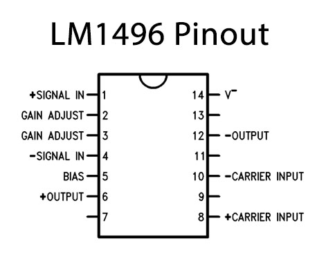
LM1496 Pinout

LM1496 Pin Configuration
| Pin No | Pin Name | Description |
|---|---|---|
| 1 | +SIGNAL IN | Positive Input Signal |
| 2 | GAIN ADJUST | Gain Adjust Pin |
| 3 | GAIN ADJUST | Gain Adjust Pin |
| 4 | -SIGNAL IN | Negative Input Signal |
| 5 | BIAS | Bias Pin |
| 6 | +OUT | Positive Output Pin |
| 7 | NC | No Connection |
| 8 | +CARRIER IN | Positive Carrier Input |
| 9 | NC | No Connection |
| 10 | -CARRIER IN | Negative Carrier Input |
| 11 | NC | No Connection |
| 12 | -OUT | Negative Output Pin |
| 13 | NC | No Connection |
| 14 | V- | Negative Voltage |
LM1496 Features
- Excellent carrier suppression,- 65 dB typical at 0.5 MHz, – 50 dB typical at 10 MHz
- Adjustable gain and signal handling
- Fully balanced inputs and outputs
- Low offset and drift
- Wide frequency response up to 100 MHz
Application
- Suppressed carrier modulation
- Amplitude modulation
- Synchronous detection
- FM or PM detection
- Broadband frequency doubling
- Chopping.
You can download this datasheet for LM1496 Balanced Modulator/Demodulator – Datasheet from the link given below:


