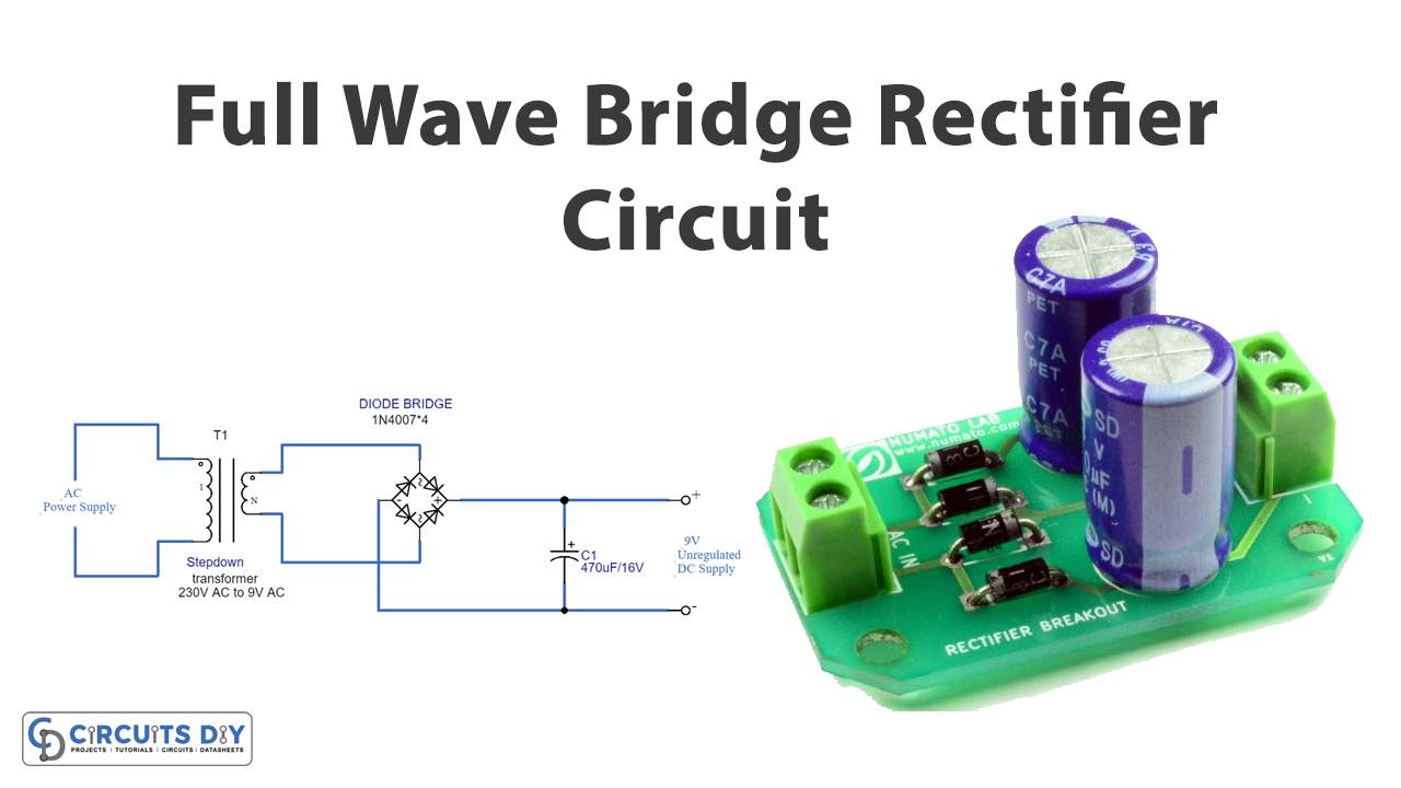
In this tutorial, we are going to make a “Full Wave Bridge Rectifier Circuit”. Many electronic circuits require a rectified DC power supply, for powering the various electronic basic components from available AC mains supply. We can find this rectifier in a wide variety of electronics. It is widely used in AC to DC converters and DC circuit designs. A full wave rectifier is called a bridge rectifier due to its shape, this type of single-phase rectifier uses four individual rectifying diodes. These diodes are connected in a closed loop “bridge” configuration, to produce the desired output.
The main advantage of this bridge circuit is that it does not require a special center-tapped transformer, thereby reducing its size and cost. The single secondary winding is connected to one side of the diode bridge network and the load to the other side. As we know that there are three ways to design a rectifier, half wave rectifier, full-wave rectifier, and bridge rectifier. But among these rectifiers, the bridge rectifier gives better efficiency and ripple-free DC.
Circuit Diagram
Working details of Bridge Rectifier
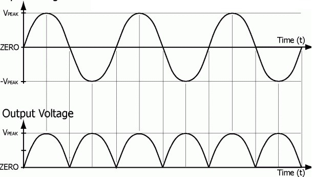
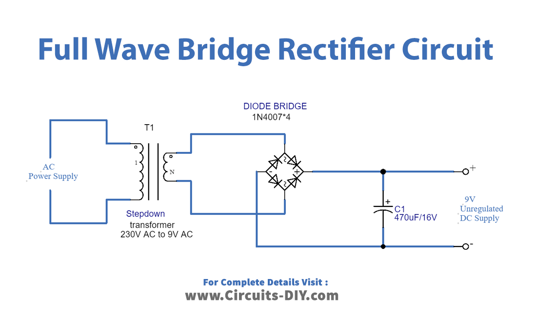
As we can see in the circuit, first the step-down transformer reduces the high voltage AC into low amplitude AC supply. Which is in form of a SINE wave, that includes both Positive and Negative cycles. As
the four diodes labeled D1 to D4 are arranged in “series pairs”, with only two diodes conducting current during each half cycle. Here diodes D1 and D2 are conducted in series during the positive half cycle of the supply. While diodes D3 and D4 are reverse-biased, the current flows through the load. Due to this during the positive cycle of the input signal, terminal A is positive with respect to terminal B. That’s why the current flows through the D1 diode and RL, and then the D3 diode finally reaches terminal B. And during this cycle diodes, D2 and D4 are not conducting any current supply.
Now during the negative half cycle of the supply, diodes D3 and D4 conduct in series. But diodes D1 and D2 switch “OFF”, as they now become reverse biased. The current flowing through the load is in the same direction as before. Due to this during the negative cycle of the input, terminal B is positive with respect to terminal A. And now the current flows through the D2 diode, RL, and D4 diode finally it reaches terminal A. And during this cycle diodes, D1 and D3 are not conducted. Hence for both positive and negative cycles, RL gets the current flow. So it’s called a full wave bridge rectifier.
Input and Output Waveforms
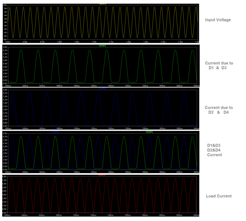
The first wave represents the input voltage, and then each diode’s output current and voltage are plotted. Finally, the load current appeared on load resistor RL. When we use a bridge rectifier, we can get continuous load current and voltage.
Some Characteristics for Reference
- Efficiency:- 81.6%
- DC Output Current:- 2Im/Π
- RMS Current:- 1m/√2
- Peak Inverse Voltage:- Vm
- Ripple factor:- 0.483
- Ripple frequency:- 2fin
- Transformer Utilization Factor:- 0.812
Working Explanation
The bridge rectifier circuit diagram consists of various stages of devices, like a transformer, diode bridge, filtering, and regulators. Generally, a combination of all these blocks is called a regulated DC power supply.
At the end of the bridge rectifier, we get a pulsating DC voltage with many ripples. We cannot use this pulsating output for practical applications. Here to convert the pulsating DC voltage to pure DC voltage, we use a filter circuit as shown below. We place a capacitor across the load. The capacitive filter circuit is placed, to short the ripples and blocks the DC component. So that it flows through another path, and is available across the load. When we apply an input AC voltage that happens to be more than the capacitor voltage, it charges the capacitor immediately to the maximum value of the input voltage. At this point, the supply voltage is equal to the capacitor voltage. When the applied AC voltage starts decreasing and is less than the capacitor, the capacitor starts discharging slowly. But this is slower when compared to the charging of the capacitor. It does not get enough time to discharge entirely, and the charging starts again. So around half of the charge present in the capacitor gets discharged. This will cause the current to flow in the same direction across the load.
The first stage of the circuit is a transformer which is a step-down type, that changes the amplitude of the input voltage. The next stage is a diode bridge rectifier, which uses four or more diodes depending on the type of bridge rectifier. Since the output after the diode bridge rectifiers is of pulsating nature. And we need a pure DC, so filtering is necessary. Filtering is normally performed with one or more capacitors attached across the load. As you can observe in the circuit, wherein smoothing of the wave is performed. This capacitor rating also depends on the output voltage. The last stage of this regulated DC supply is a voltage regulator, that maintains the output voltage at a constant level.
Although we can use four individual power diodes, to make a full wave bridge rectifier. There are pre-made bridge rectifier components also available off-the-shelf in a range of different voltage and current sizes, that can be soldered directly into a PCB circuit board or be connected by spade connectors. A typical single-phase bridge rectifier with one corner cut off. This cut-off corner indicates that the terminal nearest to the corner is the positive or +ve output terminal, or lead with the opposite (diagonal) lead being the negative or -ve output lead. The other two connecting leads are for the input alternating voltage, from a transformer’s secondary winding. It is very easy to find a bridge rectifier IC, depending on your current and voltage requirements.


