Contents
hide
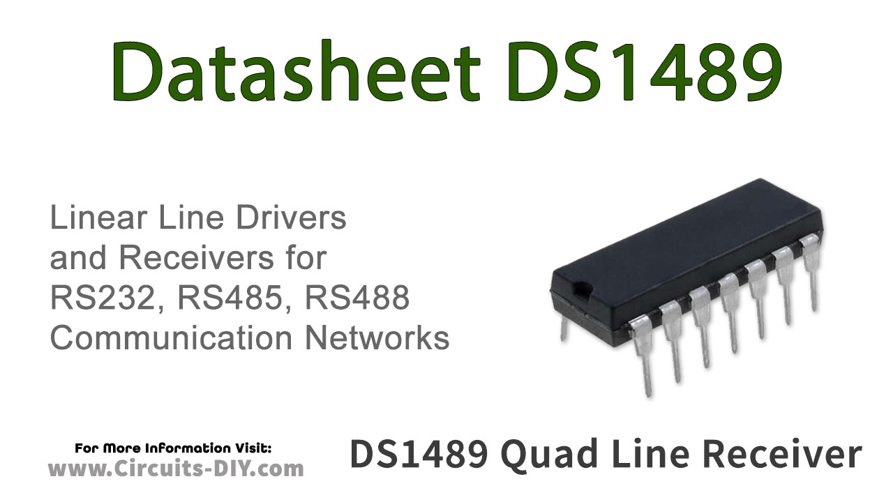
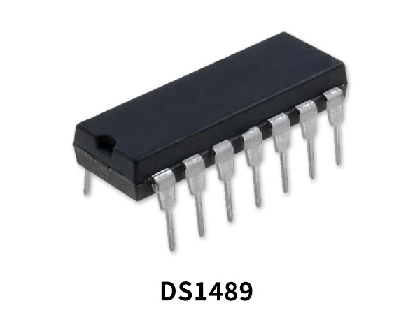
The DS1489 Quad Line Receiver (RS232) receiver is designed to interface data terminal equipment (DTE) with data circuit-terminating equipment (DCE). The device is translate levels conforming to EIA-232E and CCITT V.28 standards to TTL/CMOS logic levels. The device is fabricated in low threshold CMOS metal gate technology. The device provides very low power consumption compared to their bipolar equivalents: 900 mA (DS14C89A) versus 26 mA (DS1489A).
DS1489 Pinout
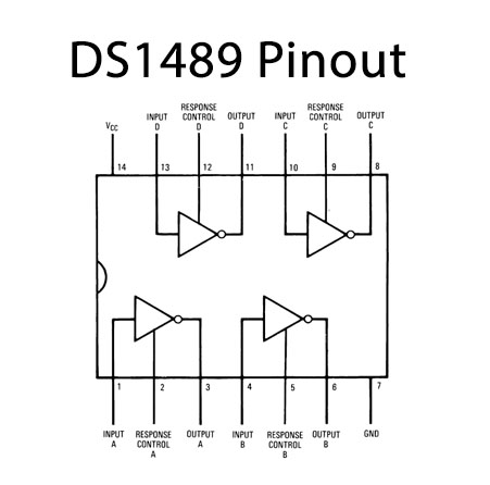
DS1489 Pin Configuration
| Pin No | Pin Name | Description |
|---|---|---|
| 1 | IN A | Input Pin A |
| 2 | RESPONSE CONTROL A | Response Control Pin A |
| 3 | OUTA | Output Pin A |
| 4 | IN B | Input Pin B |
| 5 | RESPONSE CONTROL B | Response Control Pin B |
| 6 | OUT B | Output Pin B |
| 7 | GND | Ground Pin |
| 8 | OUT C | Output Pin C |
| 9 | RESPONSE CONTROL C | Response Control Pin C |
| 10 | IN C | Input Pin C |
| 11 | OUT D | Output Pin D |
| 12 | RESPONSE CONTROL D | Response Control Pin D |
| 13 | IN D | Input Pin D |
| 14 | VCC | Collector Supply Voltage |
DS1489 Key Features
- Meets EIA/TIA-232-E and CCITT V.28 Standards
- Industrial Temperature Range 40§C to 85§C –DS14C89AT
- LOW Power consumption
- On chip noise filter
- Available in SOIC Package
You can download this datasheet for DS1489 Quad Line Receiver (RS232) from the link given below:


