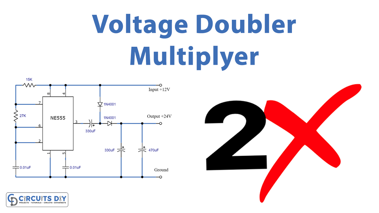
A DC Voltage Doubler/Multiplier circuit is an electronic circuit that charges capacitors from the input voltage and switches its voltages in such a way that, in an ideal case, exactly twice the voltage is produced at the output as at its input. The simplest of these circuits is a form of a rectifier that takes an AC voltage as input and outputs a doubled DC voltage. The switching elements are simple diodes and they are driven to switch state merely by the alternating voltage of the input. So, In this project, we will build a DC voltage doubler/Multiplier circuit using NE555 Timer IC.
This circuit consists of a NE555 timer IC. It gives a continuous square wave output. The circuit possesses an oscillation frequency ranging from 670 to 680 Hz.
Hardware Components
You will need the following parts to build this project.
| S.no | Component | Value | Qty |
|---|---|---|---|
| 1. | Breadboard | – | 1 |
| 2. | Power Supply | 12v | 1 |
| 3. | Connecting Wires | – | 1 |
| 4. | IC | NE555 Timer | 1 |
| 5. | Diode | 1N4001 | 2 |
| 6. | Electrolytic Capacitor | 470uF, 330uF | 1, 2 |
| 7. | Ceramic Capacitor | 0.01uF | 2 |
| 8. | Resistor | 27K, 15K | 1, 1 |
555 Timer Pinout
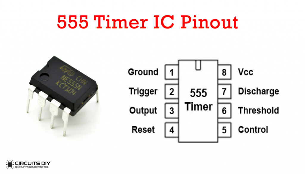
| Pin No. | Pin Name | Description |
| 1 | GND | Ground |
| 2 | TRIG | Trigger pin, set to 1/3 of Vcc |
| 3 | OUT | Timer Output |
| 4 | RESET | Reset Active Low |
| 5 | CONT | Comparator threshold control |
| 6 | THRES | Threshold pin, set to 2/3 of Vcc |
| 7 | DISCH | The low-impedance discharge path |
| 8 | Vcc | Chip supply voltages (6v-12v) |
Circuit Diagram

Working Explanation
The operation of this circuit can be broken down into two parts. The first part consists of the 555 timer IC in Astable mode, to generate the square wave and the second part consist of diodes (D1 & D2) and 2 capacitors (C3 & C4) to double the output voltage.
When the output at Pin 3 of NE555 IC is low, diode D1 gets forward biased and capacitor C3 gets charged through the diode D1. Capacitor C3 (330uF) gets charged up to the same voltage as the source, which is 12V in our case. Now when output at PIN 3 goes high, D1 gets reverse biased and blocks the discharging of the capacitor C3, and at the same time, D2 is forward biased and allows the capacitor C4 (470uF) to charge. Now the capacitor C4 (470uF) charges with the combined voltage of Capacitor C3 and the input source voltage means 12V of capacitor C3 and 12V of input supply, so it charges up to approx. 24V
Applications
- They serve in many electrical and electronic applications such as in microwave ovens, strong electric field coils for cathode-ray tubes, electrostatic and high voltage test equipment, etc.