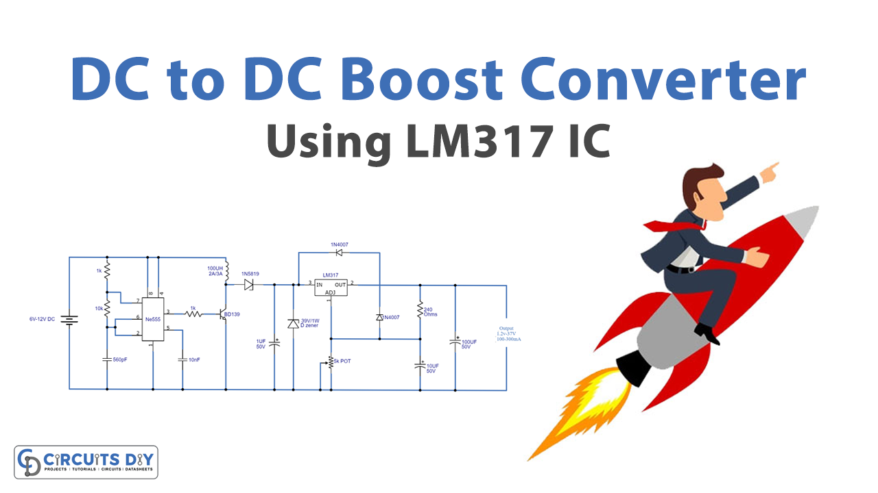
A DC to DC Adjustable Boost converter/power supply is an electronic device capable of converting a source of direct current (DC) from one voltage level to another. They fulfill a wide array of requirements in industrial as well as academic settings such as test bench supplies and load matching applications for variable DC drives. So, in this project, we are going to design a DC to DC Adjustable Step Up Boost Power Supply/ Converter using a NE555 Timer IC combined with an LM317T Voltage regulator.
Here, the Converter power supply operates by combining a few key elements. A 555-timer IC operating in astable multivibrator mode. A 39V 1W Zener diode provides a max output voltage range of 37V, and an LM317T voltage regulator IC ensures a smooth DC output. The LM317T IC removes any DC discrepancies. That might have occurred due to the Zener diode.
Hardware Components
The following components are required to make an Adjustable Boost Converter Circuit
| S.no | Component | Value | Qty |
|---|---|---|---|
| 1. | IC | NE555 Timer | 1 |
| 2. | NPN Transistor | BD139 | 1 |
| 3. | Voltage Regulator IC | LM317T | 1 |
| 4. | 1W Zener Diode | 39V/1W | 1 |
| 5. | Diode | 1N4007, 1N5819 | 1 |
| 6. | DC Supply | 6V-12V | 1 |
| 7. | Potentiometer | 5K Ohm | 1 |
| 8. | Inductor | 100uH 2A/3A | 1 |
| 9. | Electrolytic Capacitors | 100uF/50V,10uF/50V, 1uF/50V | 1 |
| 10. | Ceramic Capacitors | 10nF, 560pF | 1 |
| 11. | Resistors | 1K, 10K, 240 Ohm | 4 |
| 12. | Connecting Wires | – | As per need |
| 13. | Battery Clips | – | 1 |
| 14. | Breadboard | – | 1 |
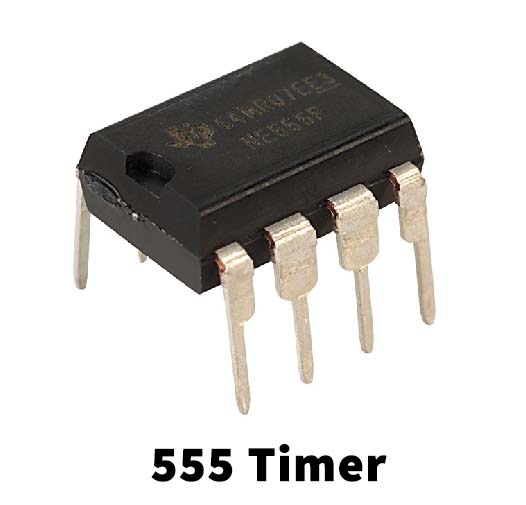
NE555 IC Pinout
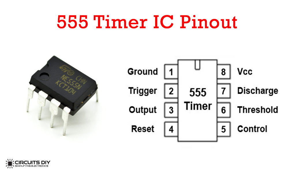
For a detailed description of pinout, dimension features, and specifications download the datasheet of NE555 IC
LM317T Pinout
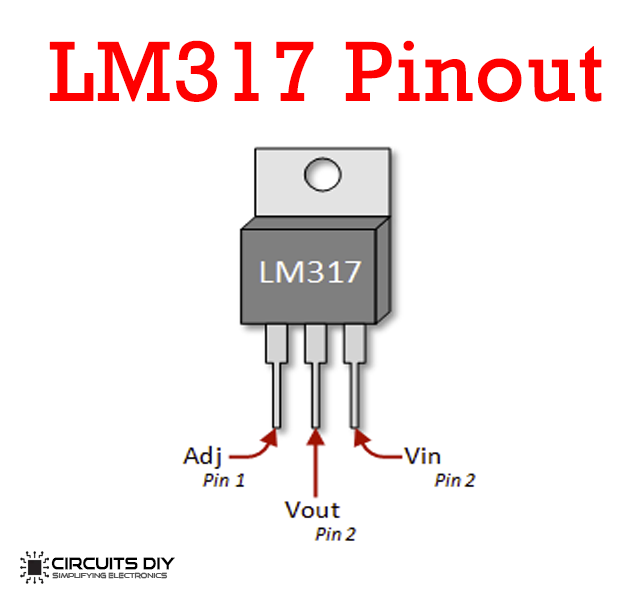
For a detailed description of pinout, dimension features, and specifications download the datasheet of LM317T
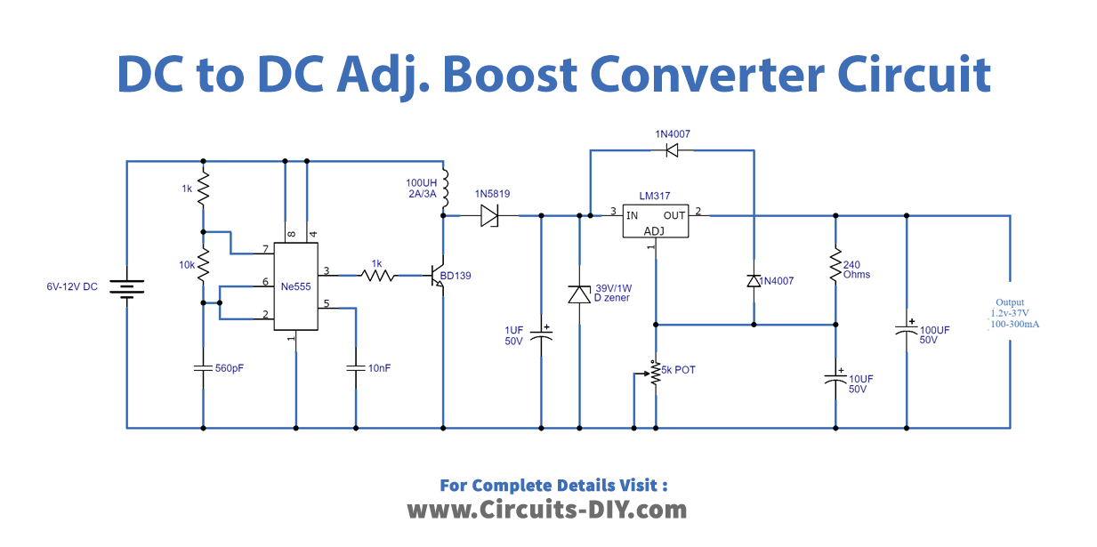
Adjustable Boost Converter Circuit
Working Explanation
The circuit is divided into two parts, the first part is a DC to DC step-up converter/booster circuit built around a 555 timer IC which boosts the input voltage to around 50V. here, the 555 timer IC is operating in astable mode. Providing a constant square wave signal. This square wave signal acts as a control signal on the base BD139 transistor.
The second part of the circuit is an adjustable power supply built with an LM317T adjustable voltage regulator IC. The regulator IC ensures a constant DC output & filters out any remaining residual noise. The 39V/1W Zener diode is used to step down the voltage coming from the booster circuit to convert it under the max input voltage limit of the LM317T IC of 40V DC. The output of the circuit can be adjusted from 1.2V to 37V DC, the max output current of the circuit ranges from 100mA to 300mA, depending on the input supply voltage.
Applications
- They commonly serve in appliances such as automobiles, portable chargers, and portable DVD players.