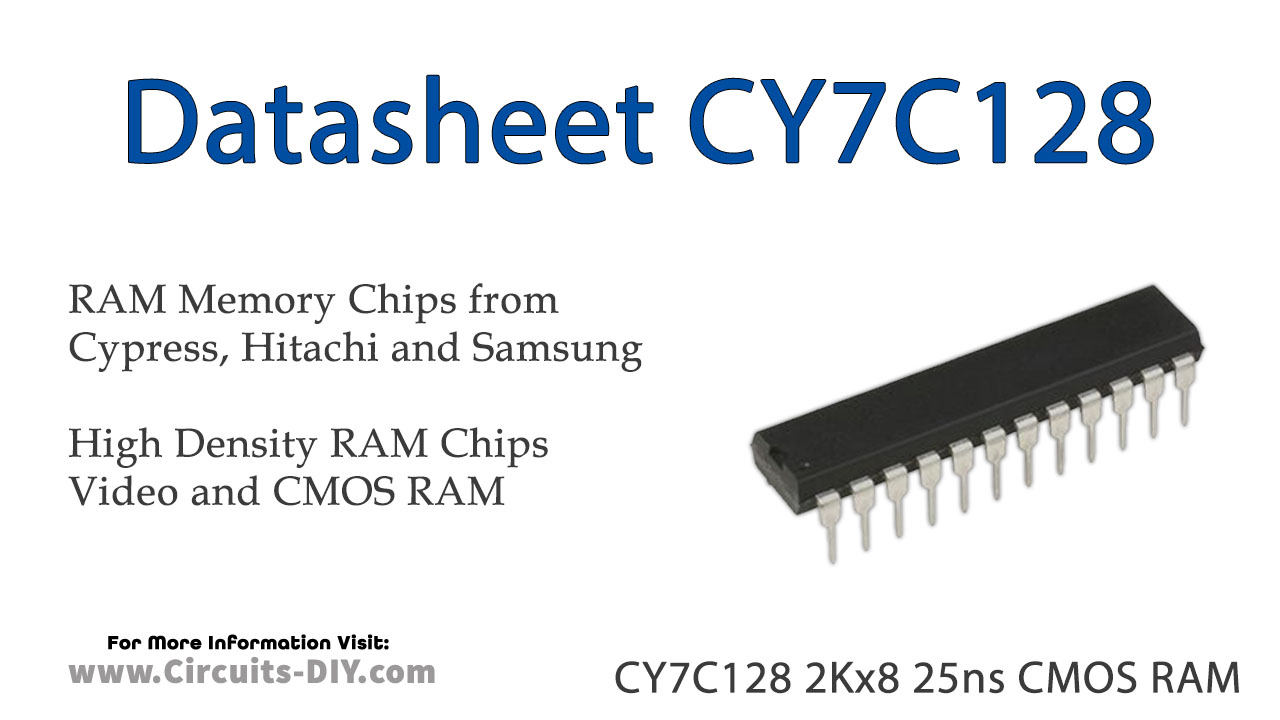
The CY7C128A is a high-performance CMOS static RAM organized as 2048 words by 8 bits. Easy memory expansion is provided by an active LOW chip enable (CE), and active LOW output-enable (OE), and three-state drivers. The CY7C128A has an automatic power-down feature, reducing the power consumption by 83% when deselected. Writing to the device is accomplished when the chip enable (CE) and write-enable (WE) inputs are both LOW. Data on the eight I/O pins (I/O0 through I/O7) is written into the memory location specified on the address pins (A0 through A10). Reading the device is accomplished by taking chip to enable (CE) and output-enable (OE) LOW while write enable (WE) remains HIGH. Under these conditions, the contents of the memory location specified on the address pins will appear on the eight I/O pins.
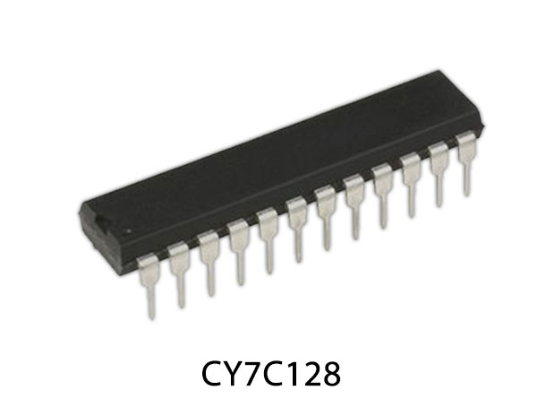
CY7C128 Pinout
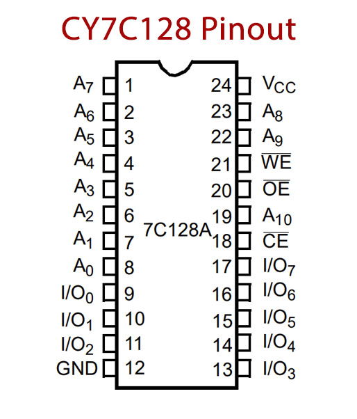
CY7C128 Pin Configuration
| Pin No | Pin Name | Description |
|---|---|---|
| 1 | A7 | Address Pin 7 |
| 2 | A6 | Address Pin 6 |
| 3 | A5 | Address Pin 5 |
| 4 | A4 | Address Pin 4 |
| 5 | A3 | Address Pin 3 |
| 6 | A2 | Address Pin 2 |
| 7 | A1 | Address Pin 1 |
| 8 | A0 | Address Pin 0 |
| 9 | I/O 0 | Data Inputs/Outputs 0 |
| 10 | I/O 1 | Data Inputs/Outputs 1 |
| 11 | I/O 2 | Data Inputs/Outputs 2 |
| 12 | GND | Ground Pin |
| 13 | I/O 3 | Data Inputs/Outputs 3 |
| 14 | I/O 4 | Data Inputs/Outputs 4 |
| 15 | I/O 5 | Data Inputs/Outputs 5 |
| 16 | I/O 6 | Data Inputs/Outputs 6 |
| 17 | I/O 7 | Data Inputs/Outputs 7 |
| 18 | CS’ | Chip Select Pin |
| 19 | A10 | Address Pin 10 |
| 20 | OE’ | Output Enable Pin |
| 21 | WE’ | Write Enable Pin |
| 22 | A9 | Address Pin 9 |
| 23 | A8 | Address Pin 8 |
| 24 | VCC | Power Supply Pin |
CY7C128 Key Feature
- Automatic power-down when deselected
- CMOS for optimum speed/power
- High speed
- 15 ns
- Low active power
- 440 mW (commercial)
- 550 mW (military)
- Low standby power
- 110 mW
- TTL-compatible inputs and outputs
- Capable of withstanding greater than 2001V electrostatic discharge
- VIH of 2.2V
You can download this datasheet for CY7C128 2Kx8 25ns CMOS RAM – Datasheet from the link given below:

