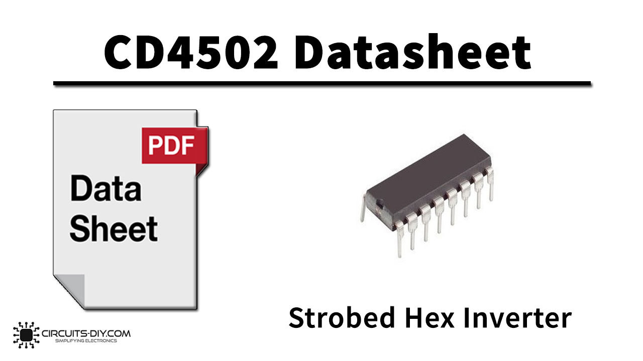
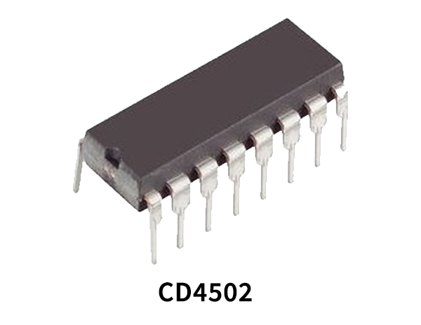
CD4502 belongs to the family of the CD4000 IC series. CD4502 Strobed Hex Inverter/Buffer, consisting of six inverter/buffers with 3 state outputs. A logic “1” on the OUTPUT DISABLE input produces a high impedance state in all six outputs. This feature permits the common busing of the outputs, thus simplifying system design. A Logic “1” on the INHIBIT input switches all six outputs to logic “0” if the OUTPUT DISABLE input is a logic “0”. The IC also offers features such as high noise immunity and ESD protection. CD4502 is always available in a 16-pin hermetically sealed IC package, allowing it to be easily interfaced with NMOS, CMOS, and TTL devices.
Hex Inverter
A Hex inverter gate inverts the input digital signal. A hex inverter always has high or logic level 1 output when its input is low or at logic level 0, and a low or logic level 0 output when input is high or at logic level 1.
Hex Buffer
A Hex buffer is a logic gate that passes its input, unchanged, to its output. Its behavior is the opposite of a hex inverter. The main purpose of a buffer is to regenerate the input. A buffer has one input and one output; its output is always equal to its input. Buffers are also used to increase the propagation delay of circuits by driving the large capacitive loads.
CD4502 Key Features
- High Voltage Type (20V Rating)
- 2 TTL Load Output Drive Capability
- 3 State Outputs
- Common Output Disable Control
- Inhibit Control
- 100% Tested for Quiescent Current at 20V
- 5V, 10V and 15V Parametric Ratings
- Maximum Input Current of 1µA at 18V Over Full Package Temperature Range; 100nA at 18V and +25oC
- Noise Margin (Over Full Package/Temperature Range)
- 1V at VDD = 5V
- 2V at VDD = 10V
- 2.5V at VDD = 15V
CD4502 Pinout
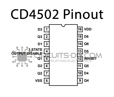
| Pin No | Pin Name | Description |
|---|---|---|
| 1 | D3 | Input Inverter 3 |
| 2 | Q3 | Output Inverter 3 |
| 3 | D1 | Iutput Inverter 1 |
| 4 | 3 STATE OUTPUT DISABLE | 3 STATE OUTPUT DISABLE |
| 5 | Q1 | Output Inverter 1 |
| 6 | D2 | Input Inverter 2 |
| 7 | Q2 | Output Inverter 2 |
| 8 | VSS | Source Supply |
| 9 | Q4 | Output Inverter 4 |
| 10 | D4 | Input Inverter 4 |
| 11 | Q5 | Output Inverter 5 |
| 12 | INHIBIT | Inhibit Pin |
| 13 | D5 | Input Inverter 5 |
| 14 | Q6 | Output Inverter 6 |
| 15 | D6 | Input Inverter 6 |
| 16 | VDD | Drain Supply |
Application
- 3 State Hex Inverter for Interfacing ICs with Data Buses
- COS/MOS to TTL Hex Buffer
CD4502 Datasheet
You can download the datasheet for CD4502 strobed Hex Inverter/Buffer IC from the link given below:
See Also: CD4556 Dual Binary 1 of 4 Decoder Inverter – Datasheet | CD4521 24-Stage Frequency Divider – Datasheet | CD4538 Dual Precision Monostable Multivibrator – Datasheet


