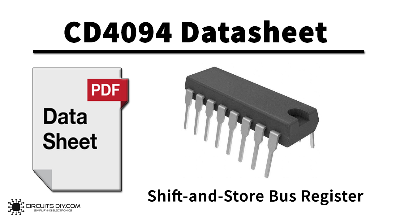
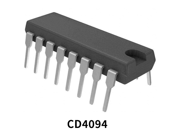
CD4094 belongs to the CD4000 IC series. It is composed of an 8-bit shift register and a 3- State 8-bit latch. Data is shifted serially through the shift register on the positive transition of the clock. The CD4094 IC has a wide range of working voltage, a wide range of working conditions, and directly interfaces with CMOS, NMOS, and TTL. The output of the IC always comes in TTL which makes it easy to work with other TTL devices and microcontrollers.
Shift-and-Store Bus Register
Shift-and-Store Bus Register are digital memory circuitry found in devices such as calculators, computers, and data processing systems. The Shift-and-Store Bus Registers allow serial or parallel data to be entered into the system. Data entry is always done from one direction, and as more data is added, it shifts positions until the data gets to the output end. The two ends are referred to as the left and right end. The movement of data can be from left to right, from right to left, or in both directions to make a bidirectional register.
CD4094 Key Features
- Wide supply voltage range: 3.0V to 18V
- High noise immunity: 0.45 VDD (typ.)
- Low power TTL compatibility:
- Fan out of 2 driving 74L or 1 driving 74LS
- 3-STATE outputs
CD4094 Pinout

| Pin No | Pin Name | Description |
|---|---|---|
| 1 | STROBE | Strobe Pin |
| 2 | DATA | Serial Data Input Pin |
| 3 | CLOCK | Shift Register Clock Pin |
| 4 | Q1 | Shift Register Output Pin 1 |
| 5 | Q2 | Shift Register Output Pin 2 |
| 6 | Q3 | Shift Register Output Pin 3 |
| 7 | Q4 | Shift Register Output Pin 4 |
| 8 | VSS | Source Supply |
| 9 | Qs | Store Register Output |
| 10 | Q’s | Store Register Inverted Output |
| 11 | Q8 | Shift Register Output Pin 8 |
| 12 | Q7 | Shift Register Output Pin 7 |
| 13 | Q6 | Shift Register Output Pin 6 |
| 14 | Q5 | Shift Register Output Pin 5 |
| 15 | ENB-OUT | enables outputs if set high |
| 16 | VDD | Drain Supply |
Application
- Serial-to-Parallel data conversion
- Remote control holding register
- Dual rank shift, hold and bus register
CD4094 Datasheet
You can download the datasheet for CD4094 8-stage Shift-and-Store Bus Register from the link given below:
See Also: 74LS74 D-Type Positive Edge Triggered Flip-Flop | 74LS91 8-Bit Shift Storage Register | 74LS95 4-Bit Shift Register IC with Parallel I/O


