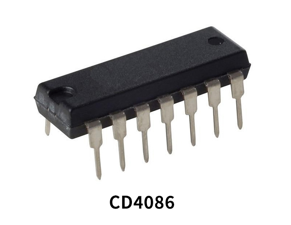
CD4086 is a part of the CD4000 IC series. CD4086 IC is a 4-wide 2-input AND-OR-INVERT gate with an INHIBIT/EXP input and an ENABLE/EXP input. The IC offers a wide array of workable voltages and operating conditions. The IC offers features such as high noise immunity and ESD barring. The CD4086B types are supplied in 14-lead hermetic dual-in-line ceramic packages. The output of CD4086 is always available in TTL, making it easy to interface with other NMOS, CMOS, and TTL devices.
AND Gate
An AND is a simple digital logic gate readily used in digital logic design. An AND gate always yields a logical HIGH when all the inputs to the AND gate are HIGH. If even a single input to the AND Gate is low the will yield a logical LOW.

OR Gate
OR gate is a digital logic gate that yields a HIGH output if even a single gate is at a HIGH Logic. In order to yield a logical LOW from an OR gate, turn any one of the inputs to LOW logic.

NOT Gate
A NOT gate is also reffered to as an invert gate. IF the input to a NOT gate is HIGH, the output will be logical LOW. Similarly, if the input is LOW, the NOT gate will yield a Logical HIGH.

CD4086 Key Features
- Medium Speed Operation – tPHL = 90ns; tPLH = 140ns (Typ.) at 10V
- High Voltage Type (20V Rating)
- INHIBIT and ENABLE Inputs
- Buffered Outputs
- 100% Tested for Quiescent Current at 20V
- Maximum Input Current of 1µA at 18V Over Full Package Temperature Range; 100nA at 18V and +25oC
- Noise Margin (Over Full Package/Temperature Range)
- 1V at VDD = 5V
- 2V at VDD = 10V
- 2.5V at VDD = 15V
- Standardized Symmetrical Output Characteristics
- 5V, 10V and 15V Parametric Ratings
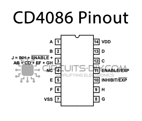
CD4086 Pinout
| Pin No | Pin Name | Description |
|---|---|---|
| 1 | A | Input 1 of AND gate 1 |
| 2 | B | Input 2 of AND gate 1 |
| 3 | Q0 | Invert output of all gates |
| 4 | NC | No Connection |
| 5 | E | Input 1 of AND gate 2 |
| 6 | F | Input 2 of AND gate 2 |
| 7 | VSS | Source Supply. |
| 8 | G | Input 1 of AND gate 3 |
| 9 | H | Input 2 of AND gate 3 |
| 10 | INHIBIT/EXP’ | INHIBIT Pin |
| 11 | ENABLE/EXP | Enable Pin |
| 12 | C | Input 1 of AND gate 4 |
| 13 | D | Input 2 of AND gate 4 |
| 14 | VDD | Drain Supply |
Application
- It is used in computer
- Calculator
- Electronic Devices.
CD4086 Datasheet
You can download the datasheet for CD4086 2-Input AND-OR-INVERT Gate from the link given below:
See Also: CD4504 Hex Voltage Level Shifter – Datasheet | CD4503 Tri-state Hex Buffer – Datasheet | CD4584 Hex Schmitt Trigger – Datasheet


