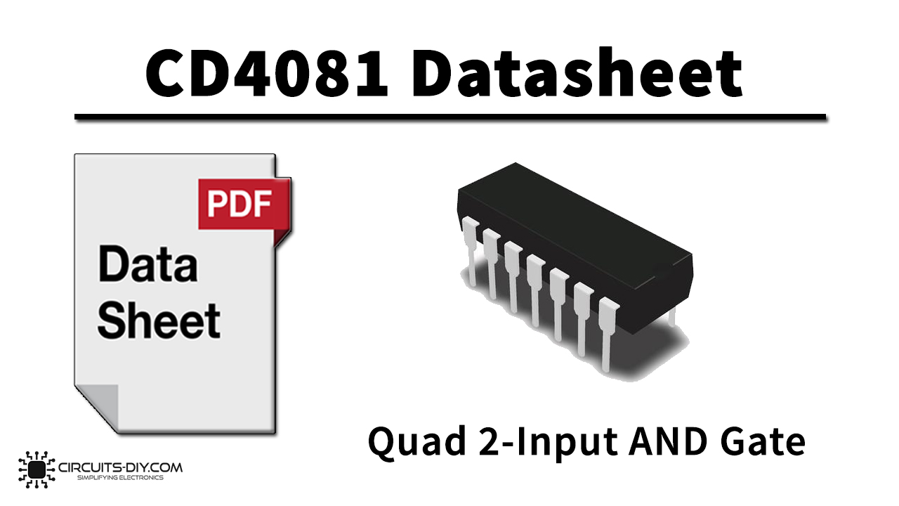
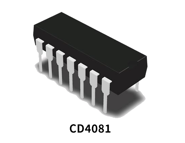
CD4081 belongs to the CD4000 IC series. CD4081 is a Quad 2-Input AND Gate designed by using the complementary MOS (CMOS) technology, integrated with N- and P-channel enhancement mode transistors. They have equal source and sink current capabilities and conform to the standard B series output drive. The IC offers many features such as thermal overload protection and high noise immunity. Every input to the IC is protected from static damage through clamping diodes. CD4081 is compact in size and easy to use making it reliable for use with any kind of device.
What is AND Gate?
An AND gate is a digital logic gate that has a plethora of applications when it comes to digital logic design. An AND gate always yield a logical HIGH, if each and every input to the AND gate remains HIGH. If even single input to the AND gate goes low then the output will also go LOW.

CD4081 Key Features
- Low power TTL compatibility:
- Fan out of 2 driving 74L or 1 driving 74LS
- 5V–10V–15V parametric ratings
- Symmetrical output characteristics
- Maximum input leakage 1 µA at 15V over full temperature range
CD4081 Pinout

| Pin No | Pin Name | Description |
|---|---|---|
| 1 | A | input 1 of AND gate 1 |
| 2 | B | input 2 of AND gate 1 |
| 3 | Q0 | output of AND gate 1 |
| 4 | Q1 | output of AND gate 2 |
| 5 | C | input 1 of AND gate 2 |
| 6 | D | input 2 of AND gate 2 |
| 7 | VSS | Source Supply |
| 8 | E | input 1 of AND gate 3 |
| 9 | F | input 2 of AND gate 3 |
| 10 | Q2 | output of AND gate 3 |
| 11 | Q3 | output of AND gate 4 |
| 12 | G | input 1 of AND gate 4 |
| 13 | H | input 2 of AND gate 4 |
| 14 | VDD | Drain supply, |
Application
- Enable gate
- Inhibit gate
- Measurement of frequency
CD4081 Datasheet
You can download the datasheet for CD4081 from the link given below:
See Also: CD4504 Hex Voltage Level Shifter – Datasheet | CD4521 24-Stage Frequency Divider – Datasheet | CD4555 Dual Binary 1 of 4 Decoder – Datasheet


