CD4073 IC is a Triple 3-input AND Gate made by using the complimentary MOS (CMOS) technology integrated with P and N type MOSFETS. This IC allows system designers to utilize the AND gate function and supplement the existing family of CMOS gates. The IC offers a wide array of workable voltages and conditions making it easy to use with different DLD configurations. The output of the IC is always available in TTL, allowing it to be easily interfaceable with CMOS, NMOS, and other TTL devices.
What is AND Gate?
AND is a basic digital logic gate that is readily utilized to implement the AND function in digital circuits. An AND gate will yield a high output (1), if all of its input are at a HIGH state. On the other hand, an AND gate will yield a LOW out put if even one of its input goes to LOW state.

CD4073 Key Features
- High-Voltage Types (20V Rating)
- CD4073BMS Triple 3-Input AND Gate
- CD4081BMS Quad 2-Input AND Gate
- CD4082BMS Dual 4-Input AND Gate
- Medium Speed Operation: tPLH, tPHL = 60ns (typ) at VDD = 10V
- 100% Tested for Quiescent Current at 20V
- Maximum Input Current of 1µA at 18V Over Full Package Temperature Range; 100nA at 18V and +25oC
CD4073 Pinout
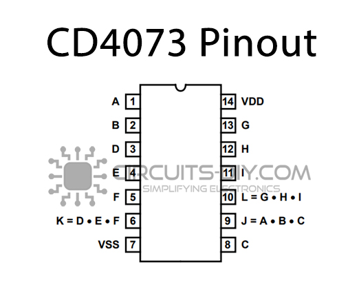
| Pin No | Pin Name | Description |
|---|---|---|
| 1 | A0 | Input Pin 0 of AND Gate 1 |
| 2 | A1 | Input Pin 1 of AND Gate 1 |
| 3 | B0 | Input Pin 0 of AND Gate 2 |
| 4 | B1 | Input Pin 1 of AND Gate 2 |
| 5 | B2 | Input Pin 2 of AND Gate 2 |
| 6 | Q1 | The output of AND Gate 2 |
| 7 | VSS | Source Supply |
| 8 | A2 | input pin 2 of AND Gate 1 |
| 9 | Q0 | The output of AND Gate 1 |
| 10 | Q2 | The output of AND Gate 3 |
| 11 | C0 | Input Pin 0 of AND Gate 3 |
| 12 | C1 | Input Pin 1 of AND Gate 3 |
| 13 | C2 | Input Pin 2 of AND Gate 3 |
| 14 | VDD | Drain Supply |
Application
- Measurement of frequency
- Enable gate and Inhibit gate
CD4073 Datasheet
You can download the datasheet for CD4073 Triple 3-input AND Gate from the link given below:
See Also: CD4504 Hex Voltage Level Shifter – Datasheet | CD4521 24-Stage Frequency Divider – Datasheet | CD4555 Dual Binary 1 of 4 Decoder – Datasheet