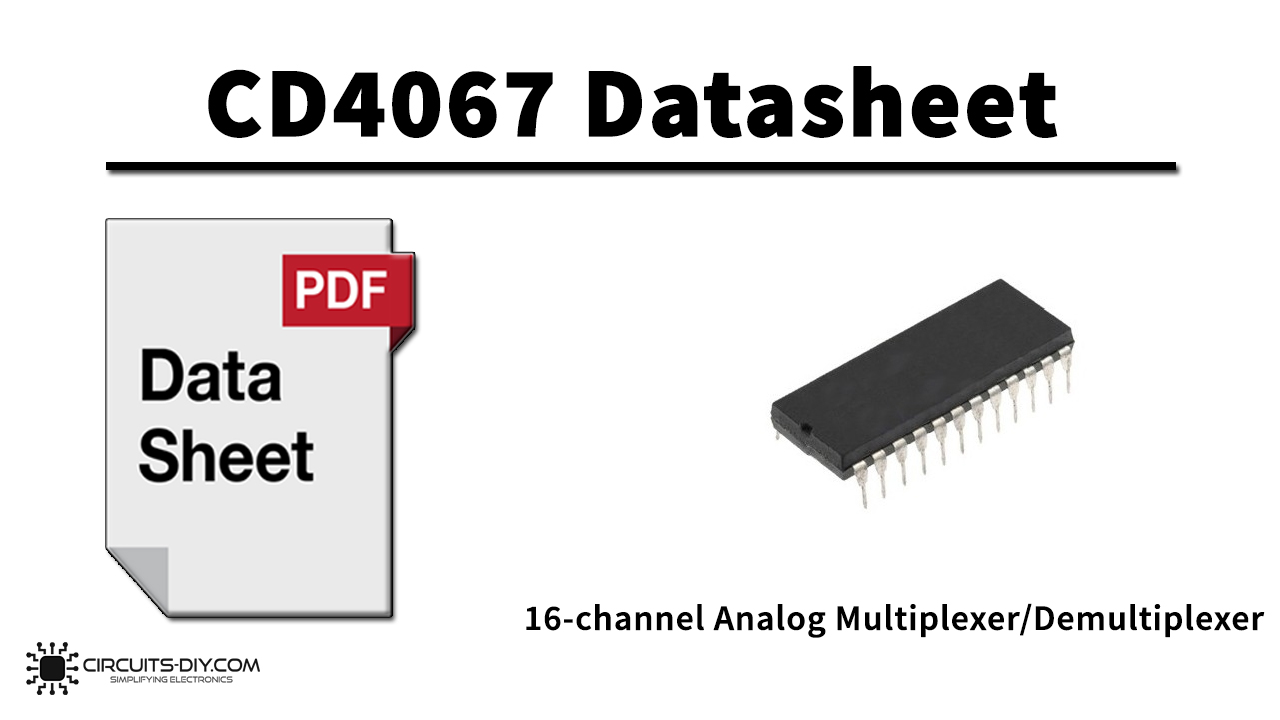
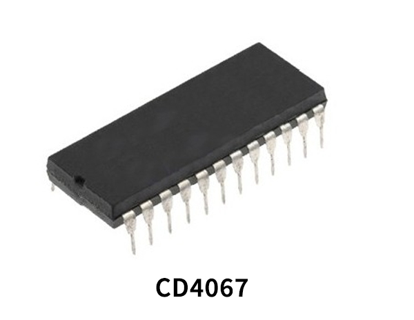
CD4067 is a part of the CD4000 IC series. CD4067 CMOS analog multiplexers/DE multiplexers are digitally controlled analog switches having low ON impedance, low OFF leakage current, and internal address decoding. The CD4067 is a 16-channel multiplexer with four binary control inputs, A, B, C, D, and an inhibit input, arranged so that any combination of the inputs selects one switch. A logic “1” present at the inhibit input turns all channels off. The IC is designed to operate over a temperature range of 0 to 70°C. The output of the IC always comes in TTL which makes it easy to work with other TTL devices and microcontrollers. The IC also constitutes a wide array of features such as thermal overload protection & ESD protection.
Multiplexer
A multiplexer is a combinational logic circuit that switches one of several input lines to a single common output line. The select lines determine which input is connected to the output, and also to increase the amount of data that can be sent over a network within a certain time. It is also called a data selector.
Demultiplexer
A decoder/demultiplexer is a combinational logic circuit & an integral part of todays consumer scale electronics. It is designed to switch one common input line to one of several separate output lines. So, A demultiplexer converts a serial data signal at the input to a parallel data at its output lines.
CD4067 Key Features
- Very low quiescent power dissipation under all digital-control input and supply conditions: 0.2 uW (typ.) @ VDD – VSS = 10 V
- Low ON resistance: 125
 (typ.) over 15 Vp-p signal-input range for VDD – VSS = 15 V
 - High OFF resistance: channel leakage of ±10 PA (typ.) @ VDD – VSS = 10 V
- Matched switch characteristics: RON = 5
 (typ.) for VDD – VSS = 15 V
 - Binary address decoding on chip
- 5-V, 10-V, and 15-V parametric ratings
- 100% tested for quiescent current at 20 V
CD4067 Pinout
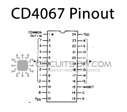
| Pin No | Pin Name | Description |
|---|---|---|
| 1 | COMMON IN-OUT PIN | Common Input / Output Pin |
| 2 | 7 | Input / Output Pin 7 |
| 3 | 6 | Input / Output Pin 6 |
| 4 | 5 | Input / Output Pin 5 |
| 5 | 4 | Input / Output Pin 4 |
| 6 | 3 | Input / Output Pin 3 |
| 7 | 2 | Input / Output Pin 2 |
| 8 | 1 | Input / Output Pin 1 |
| 9 | 0 | Input / Output Pin 0 |
| 10 | A | Selection Bit A |
| 11 | B | Selection Bit B |
| 12 | VSS | Source Supply |
| 13 | D | Selection Bit D |
| 14 | C | Selection Bit C |
| 15 | INHIBIT | Enable / Disable Signal |
| 16 | 15 | Input / Output Pin 15 |
| 17 | 14 | Input / Output Pin 14 |
| 18 | 13 | Input / Output Pin 13 |
| 19 | 12 | Input / Output Pin 12 |
| 20 | 11 | Input / Output Pin 11 |
| 21 | 10 | Input / Output Pin 10 |
| 22 | 9 | Input / Output Pin 9 |
| 23 | 8 | Input / Output Pin 8 |
| 24 | VDD | Drain supply |
Application
- Analog and digital multiplexing and demultiplexing
- A/D and D/A conversion
- Signal gating
CD4067 Datasheet
You can download the datasheet for CD4067 16-channel Analog Multiplexer/Demultiplexer IC from the link given below:
See Also: CD4504 Hex Voltage Level Shifter – Datasheet | CD4521 24-Stage Frequency Divider – Datasheet | CD4555 Dual Binary 1 of 4 Decoder – Datasheet


