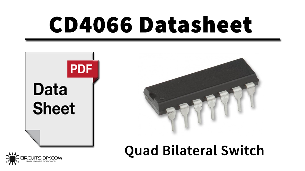
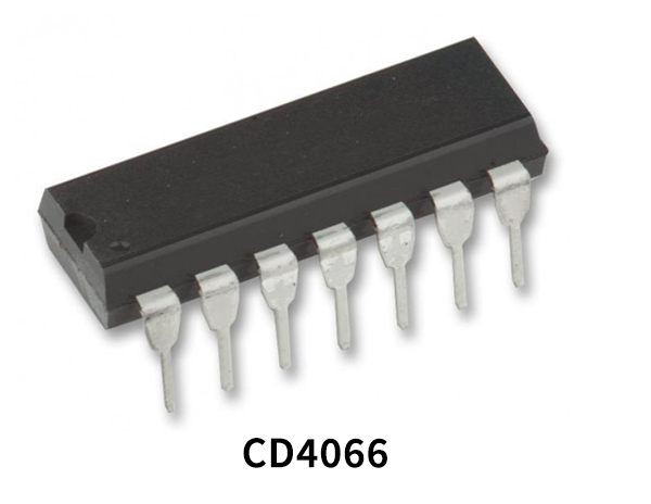
CD4066 is a part of the CD4000 IC series. The CD4066 is a quad bilateral switch intended for the transmission or multiplexing of analog or digital signals. It is pin-for-pin compatible with CD4016BC. The IC has a wide range of working voltages and conditions and has direct compatibility with CMOS, TTL, and NMOS devices. The IC offers features such as squelch controlling and ESD barring.
What is Bilateral Switch?
A Bilateral switch is an analog switch that can operate forward or reverse bias. This means that either side of the switch can be used as the input. So current can flow in one direction and the other direction, depending on which side is the input. A bilateral switch acts as a single pole, single throw switch. Each switch also has a control terminal. In order for signals to pass through from the input side to the output side, the control or enable terminal must be HIGH
CD4066 Key Features
- Wide supply voltage range 3V to 15V
- High noise immunity 0.45 VDD (typ.)
- Wide range of digital and ±7.5 VPEAK analog switching
- “ON” resistance for 15V operation 80Ω
- Matched “ON” resistance ∆RON = 5Ω (typ.)
- over 15V signal input
- “ON” resistance flat over peak-to-peak signal range
- High “ON”/“OFF” 65 dB (typ.)
- output voltage ratio @ fist = 10 kHz, RL = 10 kΩ
- Extremely high control input impedance 1012Ω(typ.)
- Low crosstalk −50 dB (typ.)
- between switches @ fist = 0.9 MHz, RL = 1 kΩ
- Frequency response, switch “ON” 40 MHz (typ.)
CD4066 Pinout
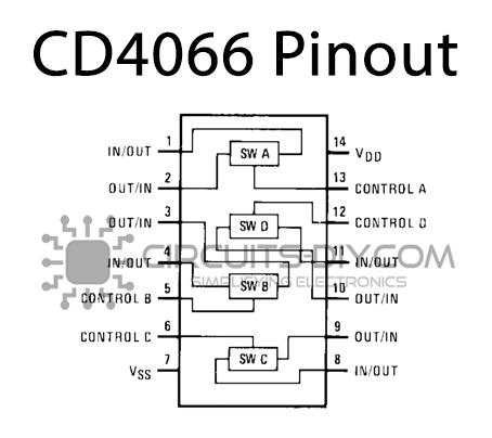
| Pin No | Pin Name | Description |
|---|---|---|
| 1 | SWA-IN | switch A input |
| 2 | SWA-OUT | switch A output |
| 3 | SWB-IN | switch B input |
| 4 | SWB-OUT | switch B output |
| 5 | CNTROL-B | control b signal |
| 6 | CNTROL-C | control c signal |
| 7 | VSS | source supply |
| 8 | SWC-IN | switch C input |
| 9 | SWC-OUT | switch C output |
| 10 | SWD-OUT | switch D output |
| 11 | SWD-IN | switch D input |
| 12 | CNTROL-D | control d signal |
| 13 | CNTROL-A | control a signal |
| 14 | VDD | Drain supply |
Application
- Analog signal switching/multiplexing
- Signal gating
- Squelch control
- Chopper
- Modulator/Demodulator
- Commutating switch
- Digital signal switching/multiplexing
- CMOS logic implementation
- Analog-to-digital/digital-to-analog conversion
- Digital control of frequency, impedance, phase, and analog-signal-gain
CD4066 Datasheet
You an download the datasheet for CD4066 Quad Bilateral Switch from the link given below:
See Also: CD4536 Programmable Timer – Datasheet | CD4527 BCD Rate Multiplier – Datasheet | CD4504 Hex Voltage Level Shifter – Datasheet