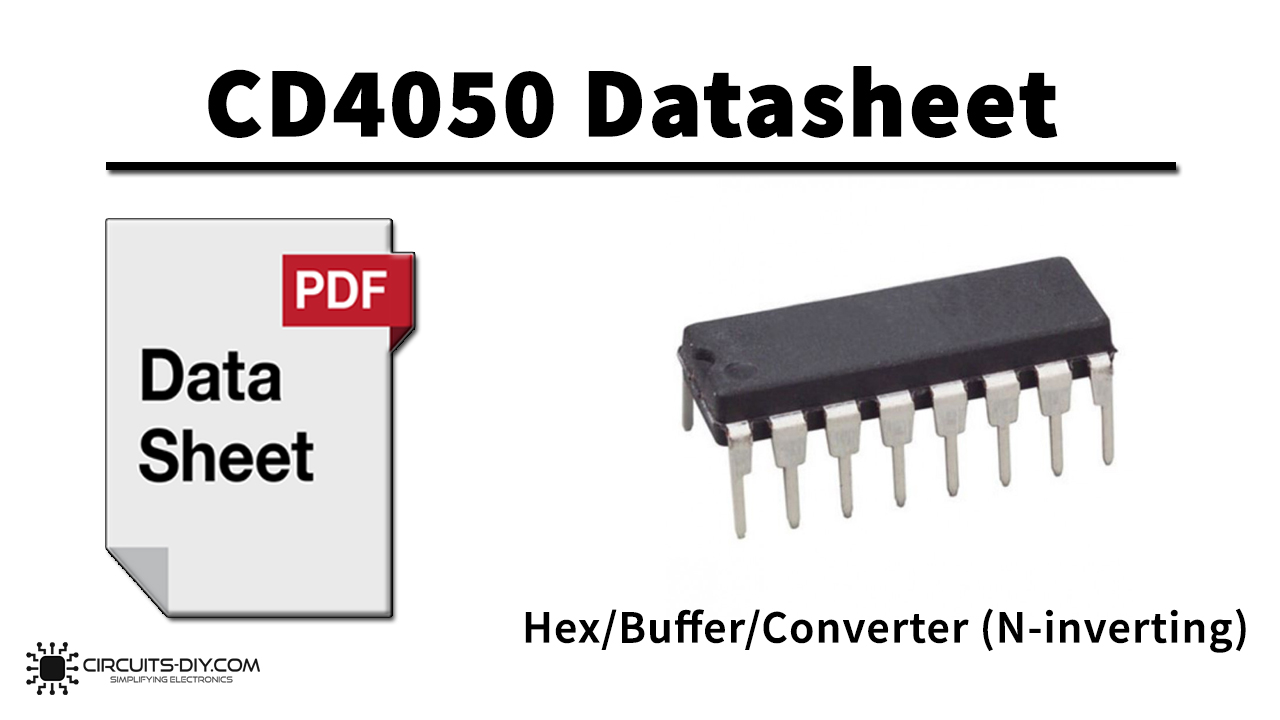
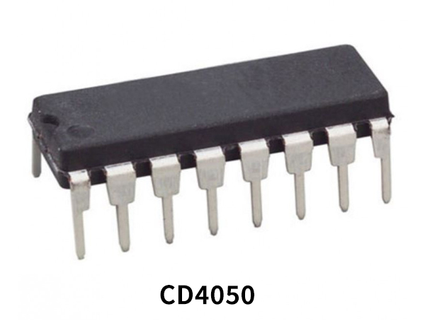
CD4050 is a hex non – inverting buffer IC belonging to the CD4000 IC series. These devices feature logic level conversion using only one supply voltage (VDD). The input signal high level (VIH) can exceed the VDD supply voltage when these devices are used for logic level conversions. These devices are intended for use as hex buffers, CMOS to DTL/ TTL converters, or as CMOS current drivers. The IC has a wide array of working conditions, operating voltages, and interfaces directly with CMOS, NMOS, and TTL devices.
What is a Non-inverting Buffer?
A non inverting buffer is a basic logic gate that passes its input, unchanged, to its output. Its behavior is the opposite of a NOT gate. The main purpose of a buffer is to regenerate the input, usually using a strong high and a strong low. A non inverting buffer has one input and one output; its output is always equal to its input. Buffers are also used to increase the propagation delay of circuits by driving the large capacitive loads.
CD4050 Key Features
- Wide supply voltage range: 3.0V to 15V
- Direct drive to 2 TTL loads at 5.0V over full temperature range
- High source and sink current capability
- Special input protection permits input voltages greater than VDD
CD4050 Pinout
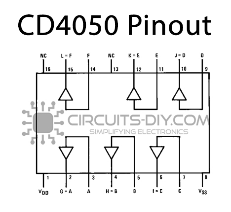
| Pin No | Pin Name | Description |
|---|---|---|
| 1 | VDD | Drain supply |
| 2 | G=A | output of non inverting buffer A |
| 3 | A | input of non inverting buffer A |
| 4 | H=B | output of non inverting buffer B |
| 5 | B | input of non inverting buffer B |
| 6 | I=C | output of non inverting buffer C |
| 7 | C | input of non inverting buffer C |
| 8 | VSS | source supply |
| 9 | D | input of non inverting buffer D |
| 10 | J=D | output of non inverting buffer D |
| 11 | E | input of non inverting buffer E |
| 12 | K=E | output of non inverting buffer E |
| 13 | NC | No connection |
| 14 | F | input of non inverting buffer F |
| 15 | L=F | output of non inverting buffer F |
| 16 | NC | No connection |
Application
- As CMOS hex inverter/buffer
- CMOS to DTL/TTL hex converter
- As CMOS current “sink” or “source” driver
- CMOS HIGH-to-LOW logic level converter
CD4050 Datasheet
You can download the datasheet for CD4050 Hex/Buffer/Converter (N-inverting) IC from the link given below:
See Also: CD4555 Dual Binary 1 of 4 Decoder – Datasheet | CD4543 BCD to 7-Segment Decoder – Datasheet | CD4541 Oscillator Programmable Timer – Datasheet

