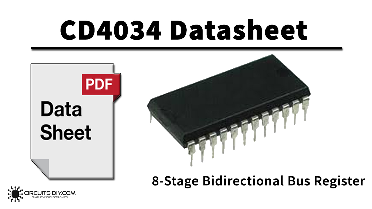
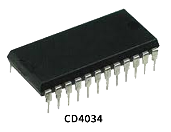
The CD4034 is an 8-bit CMOS static shift register with two parallel bidirectional data ports (A and B). The IC belongs to the CD4XXX IC series and is designed by using the complementary MOS (CMOS) technology. The output of the IC always comes in TTL, which makes it easy to interface with MCUs and MPUs. All eight register stages are D-type master-slave flip-flops with separate master and slave clock inputs generated internally to allow synchronous or asynchronous data transfer from master to slave. All inputs are protected against damage due to static discharge by diode clamps to VDD and VSS. CD4034 offers a wide variety of features such as high noise immunity and ESD protection.
What is Bus Register?
Bus registers are digital memory circuitry found in various types of equipment & tools such as calculators, computers, and data processing systems. With a shift register, data or bits are entered into the system in a serial or parallel manner. Data entry is done from one direction, and as more data is added, it shifts positions until the data gets to the output end.
CD4034 Key Features
- Wide supply voltage range 3.0V to 18V
- High noise immunity 0.45 VDD (typ.)
- Low power TTL compatibility Fan out of 2 driving 74L or 1 driving 74LS
- RCA CD4034B second source
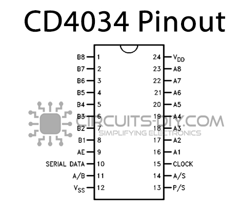
CD4034 Pinout
| Pin No | Pin Name | Description |
|---|---|---|
| 1 | B8 | DATALINE 8 OF BUS REGISTER B |
| 2 | B7 | DATALINE 7 OF BUS REGISTER B |
| 3 | B6 | DATALINE 6 OF BUS REGISTER B |
| 4 | B5 | DATALINE 5 OF BUS REGISTER B |
| 5 | B4 | DATALINE 4 OF BUS REGISTER B |
| 6 | B3 | DATALINE 3 OF BUS REGISTER B |
| 7 | B2 | DATALINE 2 OF BUS REGISTER B |
| 8 | B1 | DATALINE 1 OF BUS REGISTER B |
| 9 | “A”-EN | “A” ENABLE INPUT |
| 10 | S-INPUT | SERIAL INPUT |
| 11 | A/B | A OR B INPUT |
| 12 | VSS | source supply |
| 13 | P/S | Parallel OR Serial INPUT |
| 14 | A/S | Asynchronous OR Synchronous INPUT |
| 15 | CLK | CLOCK SIGNAL |
| 16 | A1 | DATALINE 1 OF BUS REGISTER A |
| 17 | A2 | DATALINE 2 OF BUS REGISTER A |
| 18 | A3 | DATALINE 3 OF BUS REGISTER A |
| 19 | A4 | DATALINE 4 OF BUS REGISTER A |
| 20 | A5 | DATALINE 5 OF BUS REGISTER A |
| 21 | A6 | DATALINE 6 OF BUS REGISTER A |
| 22 | A7 | DATALINE 7 OF BUS REGISTER A |
| 23 | A8 | DATALINE 8 OF BUS REGISTER A |
| 24 | VDD | Drain supply |
Application
- Parallel Input/Parallel Output
- Parallel Input/Serial Output
- Serial Input/Parallel Output
- Serial Input/Serial Output register
- Shift right/shift left register
- Shift right/shift left with parallel loading
- Address register
- Buffer register
- Bus system register with enable parallel lines at bus side
- Double bus register system
- Up-down Johnson or ring counter
- Pseudo-random code generators
- Sample and hold register (storage, counting, display)
- Frequency and phase comparator
CD4034 Datasheet
You can download the datasheet for CD4034 8-Stage Bidirectional Bus Register IC from the link given below:
See Also: CD4528 Dual Monostable Multivibrator – Datasheet | CD4067 16-channel Analog MUX/DEMUX Datasheet | CD4075 Triple 3-Input OR Gate – Datasheet


