Contents
hide
The CA3162 is an I2L monolithic A/D converter that provides a 3 digit multiplexed BCD output. This is used with the CA3161E BCD-to-Seven-Segment Decoder/Driver and a minimum of external parts to implement a complete 3-digit display. The CA3162 is identical to the CA3162AE except for an extended operating temperature range.
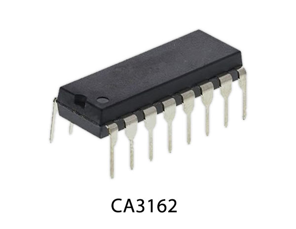
CA3162 Pinout
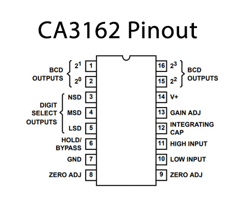
CA3162 Pin Configuration
| Pin No | Pin Name | Description |
|---|---|---|
| 1 | 2^1 | BCD Output Pin |
| 2 | 2^0 | BCD Output Pin |
| 3 | NSD | Digital Select Output Pin |
| 4 | MSD | Digital Select Output Pin |
| 5 | LSD | Digital Select Output Pin |
| 6 | HOLD/BYPASS | Hold/Bypass Pin |
| 7 | GND | Ground Pin |
| 8 | ZERO ADJ | Zero Adjust Pin |
| 9 | ZERO ADJ | Zero Adjust Pin |
| 10 | LOW IN | Low Input Pin |
| 11 | HIGH IN | High Input Pin |
| 12 | INTEGRATING CAP | Integrating Capacitor |
| 13 | GAIN ADJ | Gain Adjust Pin |
| 14 | V+ | Positive Supply Voltage Pin |
| 15 | 2^2 | BCD Output Pin |
| 16 | 2^3 | BCD Output Pin |
CA3162 Features
- Dual Slope A/D Conversion
- Multiplexed BCD Display
- Ultra Stable Internal Band Gap Voltage Reference
- Capable of Reading 99mV Below Ground with Single Supply
- Differential Input
- Internal Timing – No External Clock Required
- Choice of Low Speed (4Hz) or High Speed (96Hz) Conversion Rate
- “Hold” Inhibits Conversion but Maintains Delay
- Over range Indication
You can download this datasheet for CA3162 Dual Slope & Rate Analog/Digital Conv – Datasheet from the link given below:


