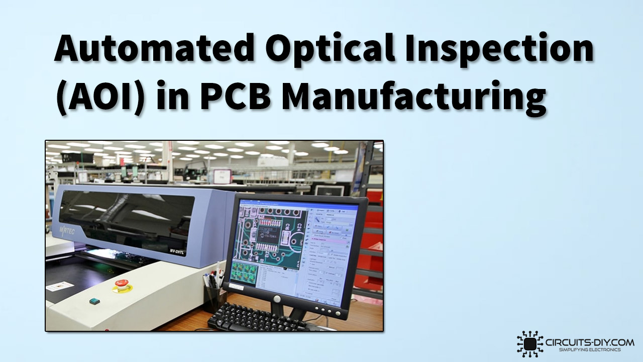
PCB assembly is a complex and intricate process; where, the result heavily depends upon how much the fabricator pays attention to detail throughout the design process. Automated optical inspection (AOI) is an important process in PCB designing and manufacturing. AOI tests play an active role in detecting the electronic assemblies and determining the operational success of PCB designs. So, in today’s article, we are going to go over the Automated optical inspection (AOI) testing system, its benefits, and its importance in PCB design and assembly.
Automated Optical Inspection (AOI)
Automated optical inspection (AOI) is an automated visual inspection of the printed circuit board (PCB) (or LCD, transistor) manufacture; where a camera autonomously scans the device under test for both catastrophic failure (e.g. missing component) and quality defects (e.g. fillet size mismatch. shape or component skewness). AOI test also checks the PCB for surface defects, dimensional defects, and component placement defects. It is commonly used in the manufacturing process because it is a non-contact test method. It is implemented at many stages through the manufacturing process including bare board inspection, solder paste inspection (SPI), pre-reflow, and post-reflow as well as other stages.

Benefits of Automated Optical Inspection (AOI)
1) Pin Point Positional Accuracy
With the decreasing technology size of PCB components, the positional accuracy of inspection equipment is becoming increasingly important. Automated optical inspection systems posses sub-pixel accuracy as a rule-of-thumb, which make sure the digital transducers is accurate enough for the system to detect the minute deviations in position that can result in a 01005 defect.

2) Cost – Effective
Using 2D and 3D AOI tests to scrutinize PCBs enhances their pass rate which ultimately contributes in decreasing the fabrication cost of the printed circuit board.

3) Operational & Inspective Versatility
AOI test not only works well used in PCBs, but also for PCB assembly. As to PCB, it checks the defects, for example, shorts, opens and insufficient solder. However, for PCB assembly, it inspects some questions, such as component soldering, polarity and values.
4) Network Oriented Software
One major benefit of AOI test is its data collection and retrieval capability. An AOI machine can retrieve and collect text output, image collection, database, or a combination of several formats. Collecting the data is a basic function of most AOI systems, but, retrieving the information is often more complex and depends on the configuration of the manufacturing line.

5) Flexible in Use
Another major advantage of using AOI testing is that it is flexible enough to be employed at any stage of the fabrication process based on the needs and cost tolerance capacity. As well as it allows immediate modification to the fabrication or assembly parameters to manufacture correctly the subsequent products.
Importance of AOI Testing
AOI testing systems offer the design safeguards that allow manufacturers to produce high quality PCBs at a profitable margin. The use of new and better AOI systems with 3D imaging feature has seen a rise due to its capability of detecting reflow soldering errors such as tombstoning and raised component pins due to poor thermal/humidity conditions in the reflow soldering process.. These errors are sometimes hard to determine by simple visual inspection or 2D AOI. Also, AOI tests maintain the quality gate for your PCB board. This makes sure that the manufacturer can provide your board conforming to all QA standards.