The ADC0817CCN data acquisition component is a monolithic CMOS device with an 8-bit analog-to-digital converter, 16-channel multiplexer and microprocessor compatible control logic. The 8-bit A/D converter uses successive approximation as the conversion technique. The converter features a high impedance chopper stabilized comparator, a 256R voltage divider with analog switch tree and a successive approximation register. The 16-channel multiplexer can directly access any one of 16-single-ended analog signals, and provides the logic for additional channel expansion. Signal conditioning of any analog input signal is eased by direct access to the multiplexer output, and to the input of the 8-bit A/D converter.
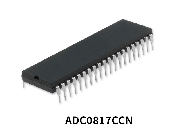
ADC0817CCN Pinout
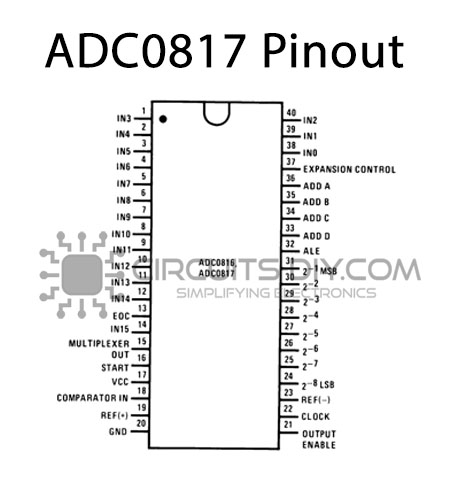
ADC0817CCN Pin Configuration
| Pin No | Pin Name | Description |
|---|---|---|
| 1 | IN3 | Analog Input Pin 3 |
| 2 | IN4 | Analog Input Pin 4 |
| 3 | IN5 | Analog Input Pin 5 |
| 4 | IN6 | Analog Input Pin 6 |
| 5 | IN7 | Analog Input Pin 7 |
| 6 | IN8 | Analog Input Pin 8 |
| 7 | IN9 | Analog Input Pin 9 |
| 8 | IN10 | Analog Input Pin 10 |
| 9 | IN11 | Analog Input Pin 11 |
| 10 | IN12 | Analog Input Pin 12 |
| 11 | IN13 | Analog Input Pin 13 |
| 12 | IN14 | Analog Input Pin 14 |
| 13 | EOC | END Of Conversion |
| 14 | IN15 | Analog Input Pin 15 |
| 15 | MULTIPLEXER OUT | Multiplexer Output Pin |
| 16 | START | Start Pin |
| 17 | VCC | Supply Voltage |
| 18 | COMPARATOR IN | Comparator Input Pin |
| 19 | REF(+) | Positive Reference Voltage |
| 20 | GND | Ground Pin |
| 21 | EN OUT | Enable Output Pin |
| 22 | CLK | Clock Pin |
| 23 | REF(-) | Negative Reference Voltage |
| 24 | 2^-8 LSB | TRI State Output Pin 8 |
| 25 | 2^-7 | TRI State Output Pin 7 |
| 26 | 2^-6 | TRI State Output Pin 6 |
| 27 | 2^-5 | TRI State Output Pin 5 |
| 28 | 2^-4 | TRI State Output Pin 4 |
| 29 | 2^-3 | TRI State Output Pin 3 |
| 30 | 2^-2 | TRI State Output Pin 2 |
| 31 | 2^-1 MSB | TRI State Output Pin 1 |
| 32 | ALE | Address Latch Enable |
| 33 | ADD D | Address Latch and Decoder Pin D |
| 34 | ADD C | Address Latch and Decoder Pin C |
| 35 | ADD B | Address Latch and Decoder Pin B |
| 36 | ADD A | Address Latch and Decoder Pin A |
| 37 | EXPANSION CNTROL | Expansion Control Pin |
| 38 | IN0 | Analog Input Pin 0 |
| 39 | IN1 | Analog Input Pin 1 |
| 40 | IN2 | Analog Input Pin 2 |
ADC0817CCN Features
- Easy interface to all microprocessors
- Operates ratiometrically or with 5 VDC or analog span adjusted voltage reference
- 16-channel multiplexer with latched control logic
- Outputs meet TTL voltage level specifications
- 0V to 5V analog input voltage range with single 5V supply
- No zero or full-scale adjust required
- Standard hermetic or molded 40-pin DIP package
- Temperature range −40°C to +85°C or −55°C to +125°C
- Latched TRI-STATE output
- Direct access to “comparator in” and “multiplexer out” for signal conditioning
ADC0817CCN Specifications
- Resolution 8 Bits
- Total Unadjusted Error ±1⁄2 LSB and ±1 LSB
- Single Supply 5 VDC
- Low Power 15 mW
- Conversion Time 100 μs
Application
- Machine control to consumer
- Automotive Applications
You can download this datasheet for ADC0817CCN 8-bit A/D Converter With 16-Ch MUX from the link given below:


