Contents
hide
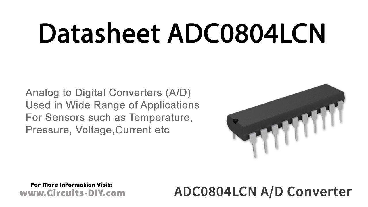
The ADC0804LCN is CMOS 8-bit successive approximation A/D converters that use a differential potentiometric ladder similar to the 256R products. These converters are designed to allow operation with the NSC800 and INS8080A derivative control bus with TRI-STATE output latches directly driving the data bus. These A/Ds appear like memory locations or I/O ports to the microprocessor and no interfacing logic is needed.
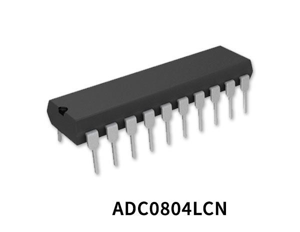
ADC0804LCN Pinout
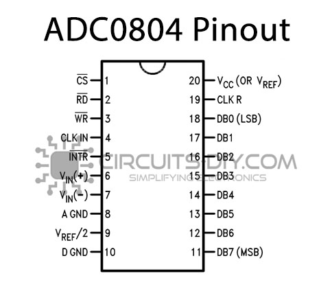
ADC0804LCN Pin Configuration
| Pin Number | Pin Name | Description |
|---|---|---|
| 1 | CS’ | Chip Select (Active Low) |
| 2 | RD’ | Read (Active Low) |
| 3 | WR’ | Write (Active Low) |
| 4 | CLK IN | Clock In |
| 5 | INTR’ | Interrupt (Active Low) |
| 6 | Vin+ | Analog Voltage Input |
| 7 | Vin- | Analog Voltage Input |
| 8 | AGND | Analog Ground |
| 9 | Vref/2 | Voltage Reference/2 |
| 10 | DGND | Digital Ground |
| 11 | DB7 | Data Bit 7 |
| 12 | DB6 | Data Bit 6 |
| 13 | DB5 | Data Bit 5 |
| 14 | DB4 | Data Bit 4 |
| 15 | DB3 | Data Bit 3 |
| 16 | DB2 | Data Bit 2 |
| 17 | DB1 | Data Bit 1 |
| 18 | DB0 | Data Bit 0 |
| 19 | CLKR | Clock Reset |
| 20 | Vcc | Positive Supply |
ADC0804LCN Features
- Compatible with 8080 µP derivatives — no interfacing logic needed – access time – 135 ns
- Easy interface to all microprocessors, or operates “stand alone”
- Differential analog voltage inputs
- Logic inputs and outputs meet both MOS and TTL voltage level specifications
- Works with 2.5V (LM336) voltage reference
- On-chip clock generator
- 0V to 5V analog input voltage range with single 5V supply
- No zero adjust required
- 0.3″ standard width 20-pin DIP package
- 20-pin molded chip carrier or small outline package
ADC0804LCN Specifications
- Resolution 8 bits
- Total error ±1⁄4 LSB, ±1⁄2 LSB and ±1 LSB
- Conversion time 100 µs
Application
- Sampling an AC Input Signal
- 3-Decade Logarithmic A/D Converter
You can download this datasheet for ADC0804LCN 8-bit A/D Converter from the link given below:


