Introduction
Whether you’re making your first PCB or building an electronic hardware product, you’ll need a PCB manufacturing service to make your hardware more accessible and faster by delivering rapid PCB prototyping and SMT assembly. So, out of hundreds of service providers, JLCPCB is the industry leader.
JLCPCB has been working to increase efficiency and save expenses since 2006. They are dedicated to consistently providing their clients with the most cost-effective PCBs from China. Because of the scale effect, exceptionally high manufacturing efficiency, and lower labor costs, JLCPCB manufactures the cheapest yet best quality PCBs. They’re always exploring methods to enhance and speed up the PCB prototype process, from inventing online quoting systems and automated production to quick turnaround.
But, how the JLCPCB is the best manufacturing company. For this, We’ll dig at what goes on behind the scenes at JLCPCB, one of the world’s leading high-quality online PCB manufacturers.
Manufacturing at JLCPCB Factory
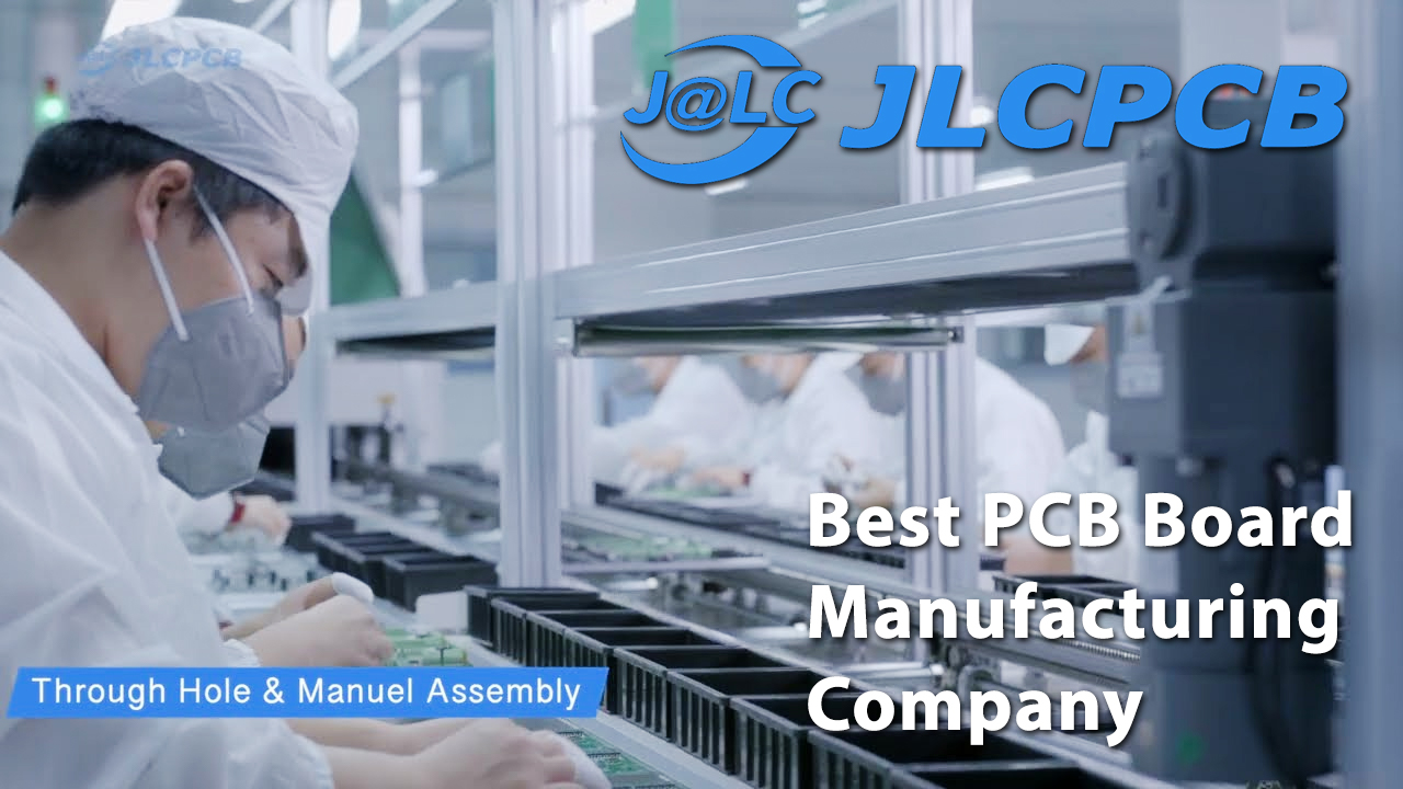
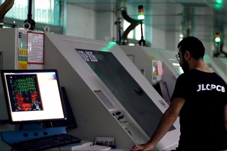
JLCPCB is a PCB manufacturer that offers a complete production cycle Everything is done under one roof, from raw materials to completed products.
Cutting
It must first cut down the printed board to a specific size following the circuit design. Clean and cut raw materials, such as copper-covered boards, to the proper size. They are then sent to the next machine for edge processing after being chopped into pieces.
Drilling
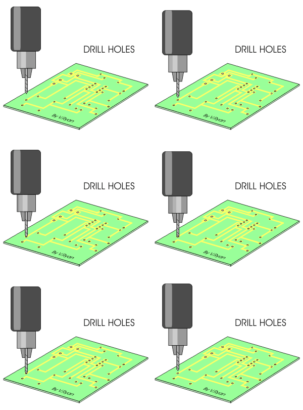
After that, the drilling procedure begins. Drilling is making holes, cavities, and other slots in a circuit board before installing electronic elements or components. They usually accomplish it with a PCB drill bit automated equipment. After the drilling, the board appears to be a bit filthy; therefore, it is cleaned with brushes.
Copper Deposition
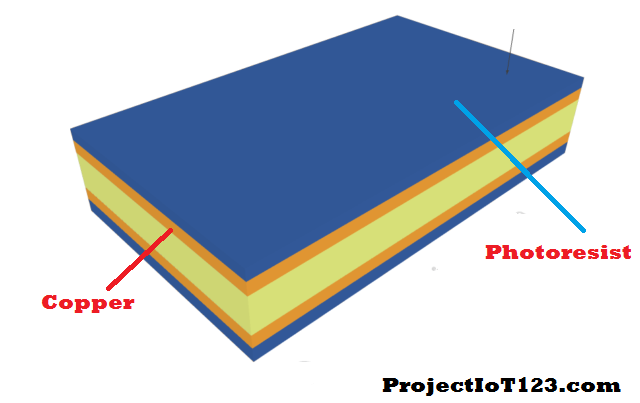
Another layer of copper is put over the boards in this step of Industrial PCB Manufacturing. This is the step at which the holes’ main metallization is generated, which is vital in producing a double-sided or multilayered PCB. These boards are washed and cleaned once again.

Photoresist
A thick coating of photoresist is applied to the board at this step. Following that, a photomask with the layout is applied over the board. The PCB layout is printed on photomasks, which are translucent sheets.
Exposure to UV Light
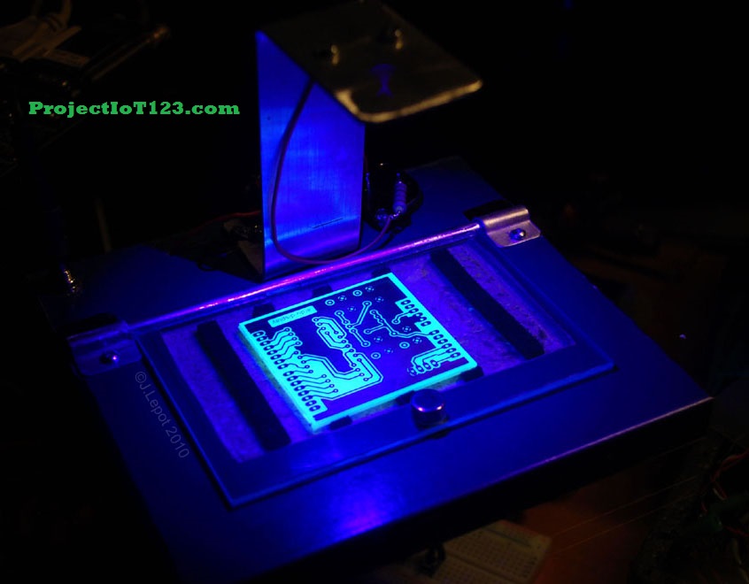
Now. The board is subjected to UV light, passing through the accessible areas. This polymerizes the region where there is no photomask.
Baking
After washing, these boards are baked in ovens to strengthen the photoresist’s mechanical robustness. The board must be baked at a specified temperature to remove moisture throughout the procedure. Following that, a slight coating of the tin-lead alloy is chemically placed on the last copper layer, boosting the hole’s dependability. They’re also put on copper rails where the photoresist had previously been removed. The only objects that remain on the final board are these. During the etching process, everything else will be gone.

Etching
PCB etching is the chemical removal of copper that hasn’t been protected. The conveyor conveys the boards, and the exposed copper is etched away using etching solutions jets. The Lead coating is removed in a similar chemical method after etching.

Error Checking
There will be some residues of undesirable lead or copper on the board. The Quality Control Center will correct all of this. Mistakes will be repaired automatically or manually under micro testing if any faults or errors are discovered. If too many faulty boards are discovered, they are entirely discarded, and replacement boards of higher quality are created.
Masking
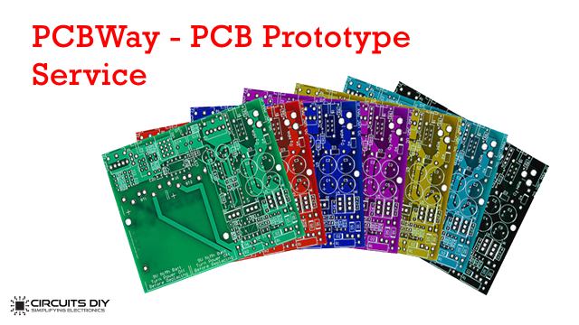
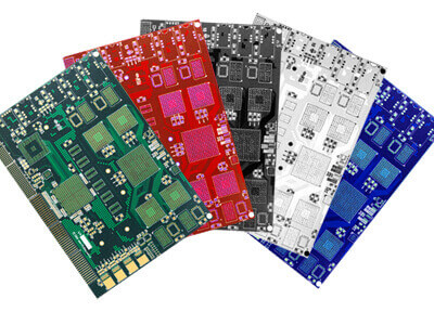
After that, there is a masking procedure. After the masking process, the green, blue, or any other color you see on boards appears. The board is protected against corrosion using this method. As a result, masking is applied to the board to protect the copper from corrosion and other potentially damaging actions. The board is given an industrial look through masking. You can choose any color for masking. The organization provides a broad array of colors, including blue, red, green, purple, and black, to mention a few.
Silk Screen Printing
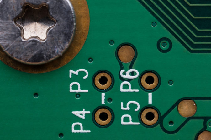
Silkscreen is a printed circuit board layer that serves as a reference or note indicator for components. It necessitates special ink, the standard color of which is white, although other colors may be used.
Surface Treatment
During this surface treatment process, an exposed surface of copper, where the component gets soldered, is coated with tin plated or gold to protect the copper from corrosion for a long time.
Testing
It’s now time to check or test the complete board. Automated equipment is used to examine all connections on a printed circuit board.
Conclusion
JLCPCB can create PCBs of varying levels of complexity. They produce both inexpensive single-layer PCBs for beginners and enthusiasts and complicated multilayer PCBs for high-quality industrial applications.

