Introduction
Are you working on a new project and need an SMT PCB designed particularly for it? Regard yourself to a fully customized PCB with SMT assembly from JLCPCB, all ready in under 24 hours just for you! We have already discussed in our various articles What is JLCPCB and what services they provide, and today in this article we are going to teach you how to place your SMT order on JLCPCB.
JLCPCB’s assembling of SMT components is more reliable and efficient. It does need a clear understanding of the technique. It also contains specifications for the design phase. SMT develops designs that are both efficient and effective. It can combine more components in a smaller space. As a result, time and money are saved, and mistakes are decreased. It does, however, continue to grow regularly. It is expected to continue to improve in the future.

Steps to place your SMT Order on JLCPCB
To place your first order on JLCPCB.COM, simply follow the simple procedures outlined below. The procedure is simple and uncomplicated to follow.
Step 1: Setup Your account
To begin, you must first create an account by signing up. After that, you may log in and begin placing your orders.

Step 2: Add Quote
A quote calculator may be found on the home page. Simply specify the size, nA quote calculator may be found on the home page. Simply specify the size, number, thickness, and layers of your chosen PCB. You may also receive a quotation by going to https://cart.jlcpcb.com/quote.
Step 3: Add a Gerber File
After that, click Add your Gerber file to begin uploading your file.
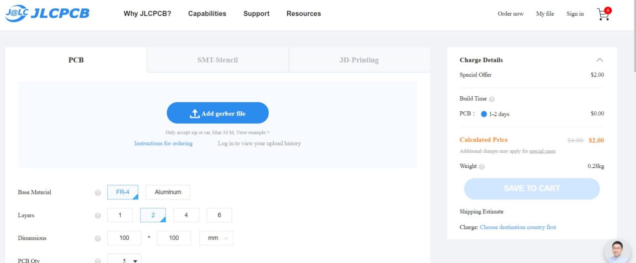
Gerber files are ASCII vector files that include information on each layer of PCB design. Copper traces, solder masks, pads, vias, and silkscreen images are all represented on a circuit board by a flash/draw code and described by a set of vector coordinates. These files are used by PCB manufacturers to convert the intricacies of your PCB design into physical attributes of the PCB.
It should go without saying that Gerber files are required for PCB fabrication. PCB manufacturers will be unable to completely comprehend the features of a PCB design file unless the PCB designer provides Gerber files since the Gerber file acts as both a reference and a guideline.
After you submit your Gerber files, their system will automatically evaluate them and determine your board dimensions and layers.

Step 3: Gerber Viewer
To see your design, click Gerber Viewer when you’re completed. It’s critical to thoroughly inspect your file for errors. To continue, simply click Save to Cart when you’re finished.

Step 4: Finalize Your Order
Repeat step for each additional PCB you wish to order by clicking Add new item. After that, proceed to your cart and complete your order.

Step 5: Shipping Information
On the following screen, you must provide your shipping address. The cost of shipping will vary depending on your location. The delivery time is 3-5 days, whereas Airmail takes 15-25 days.

Step 6: Payment Method
There are two types of payment methods available
Review before Payment: After your file review has been granted, you can pay. They will not put your design into production until they receive payment from you. They send you an email with the results.
Direct Payment: To achieve maximum production efficiency, we recommend that you pay before file evaluation. You will receive a full refund if your file cannot be authorized for production after review.

Step 6: Check Order Status
Your order will be moved to the production queue after payment is received. To check the status of your order, go to the ACCOUNT menu.

That’s all there is to it! You’ve placed your order, and it will normally be completed within 24 hours, however, it may take longer in exceptional circumstances.
Why you Need to Use SMT Assembly of JLCPCB?
SMD components and SMT technologies make it possible to:
- Electrical noise reduction
- Higher circuit density.
- Cost reduction are all advantages of complex designs.
The surface mount technique is quick and employs an automated welding procedure. As a result:
- User can save Money. Because there is no metallized hole process
- Electronic boards’ weight is being reduced.
- Saves time on manual labour and eliminates human mistakes in large-scale electronic board assembly.

