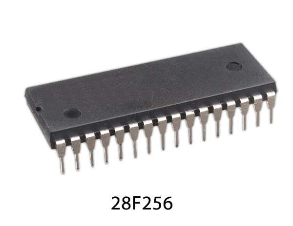
The 28F256 is a 256 K Flash memory organized as 32 Kbytes of 8 bits each. AMD’s Flash memories offer the most cost-effective and reliable read/write non-volatile random access memory.
The 28F256 is packaged in 32-pin PDIP, PLCC, and TSOP versions. It is designed to be reprogrammed and erased in-system or in standard EPROM programmers. The 28F256 is erased when shipped from the factory.
The standard 28F256 offers access times as fast as 70 ns, allowing the operation of high-speed microprocessors without wait states. To eliminate bus contention, the 28F256 has separate chip enable (CE#) and output-enable (OE#) controls. AMD’s Flash memories augment EPROM functionality with in-circuit electrical erasure and programming. The 28F256 uses a command register to manage this functionality while maintaining a standard JEDEC Flash Standard 32-pin pinout. The command register allows for 100% TTL level control inputs and fixed power supply levels during erase and programming.
28F256 Pinout
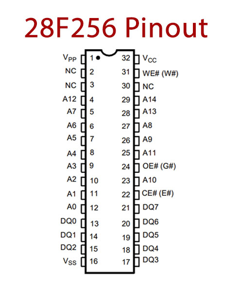
28F256 Pin Configuration
| Pin No | Pin Name | Description |
|---|---|---|
| 1 | VPP | Programming Supply |
| 2 | NC | No Connection |
| 3 | NC | No Connection |
| 4 | A12 | Address Pin 12 |
| 5 | A7 | Address Pin 7 |
| 6 | A6 | Address Pin 6 |
| 7 | A5 | Address Pin 5 |
| 8 | A4 | Address Pin 4 |
| 9 | A3 | Address Pin 3 |
| 10 | A2 | Address Pin 2 |
| 11 | A1 | Address Pin 1 |
| 12 | A0 | Address Pin 0 |
| 13 | DQ 0 | Data Output 0 |
| 14 | DQ 1 | Data Output 1 |
| 15 | DQ 2 | Data Output 2 |
| 16 | VSS | Ground Pin |
| 17 | DQ 3 | Data Output 3 |
| 18 | DQ 4 | Data Output 4 |
| 19 | DQ 5 | Data Output 5 |
| 20 | DQ 6 | Data Output 6 |
| 21 | DQ 7 | Data Output 7 |
| 22 | CE’ | Chip Enable Pin |
| 23 | A10 | Address Pin 10 |
| 24 | OE’ | Output Enable Pin |
| 25 | A11 | Address Pin 11 |
| 26 | A9 | Address Pin 9 |
| 27 | A8 | Address Pin 8 |
| 28 | A13 | Address Pin 13 |
| 29 | A14 | Address Pin 14 |
| 30 | NC | No Connection |
| 31 | WE | Write Enable Pin |
| 32 | VCC | Power Supply |
28F256 Key Feature
- High performance
- 70 ns maximum access time
- CMOS Low power consumption
- 30 mA maximum active current
- 100 µA maximum standby current
- No data retention power consumption
- Compatible with JEDEC-standard byte-wide
- 32-Pin EPROM pinouts
- 32-pin PDIP
- 32-pin PLCC
- 32-pin TSOP
- 10,000 write/erase cycles minimum
- Write and erase voltage 12.0 V ±5%
You can download this datasheet for 28F256 256k 150ns CMOS Flash Memory – Datasheet from the link given below:


