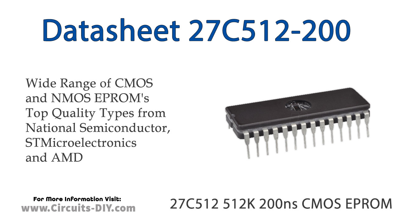
The M27C512 is a 512 Kbit EPROM offered in the two ranges UV (ultra violet erase) and OTP (one-time programmable). It is ideally suited for applications where fast turn-around and pattern experimentation are important requirements and is organized as 65,536 by 8 bits. The FDIP28W (window ceramic frit-seal package) has a transparent lid that allows the user to expose the chip to ultraviolet light to erase the bit pattern. A new pattern can then be written to the device by following the programming procedure. For applications where the content is programmed only one time and erasure is not required, the M27C512 is offered in PDIP28, PLCC32, and TSOP28 (8 x 13.4 mm) packages.

27C512 Pinout

27C512 Pin Configuration
| Pin Number | Pin No | Description |
|---|---|---|
| 1 | A15 | Address Input |
| 2 | A12 | Address Input |
| 3 | A7 | Address Input |
| 4 | A6 | Address Input |
| 5 | A5 | Address Input |
| 6 | A4 | Address Input |
| 7 | A3 | Address Input |
| 8 | A2 | Address Input |
| 9 | A1 | Address Input |
| 10 | A0 | Address Input |
| 11 | Q0 | Data Output |
| 12 | Q1 | Data Output |
| 13 | Q2 | Data Output |
| 14 | VSS | Ground |
| 15 | Q3 | Data Output |
| 16 | Q4 | Data Output |
| 17 | Q5 | Data Output |
| 18 | Q6 | Data Output |
| 19 | Q7 | Data Output |
| 20 | E’ | Chip Enable |
| 21 | A10 | Address Input |
| 22 | G’/VPP | Output Enable/Program Supply |
| 23 | A11 | Address Input |
| 24 | A9 | Address Input |
| 25 | A8 | Address Input |
| 26 | A13 | Address Input |
| 27 | A14 | Address Input |
| 28 | VCC | Positive Power Supply |
27C512 Key Features
- 5V ± 10% Supply Voltage in reading Operation
- Fast Access Time: 45ns
- Low Power “CMOS” Consumption:
- Active Current 30mA
- Standby Current 100µA
- Programming Voltage: 12.75V ± 0.25V
- Programming Times of Around 6sec.
- Electronic Signature
- Manufacturer Code: 20h
- Device Code: 3Dh
You can download this datasheet for 27C512 512K 200ns CMOS EPROM – Datasheet from the link given below:

