Introduction
In the designing of Printed circuit boards, some major factors can affect the circuit. These issues can damage the entire circuit and hence the device. The issues like acid traps starved thermal, insufficient annular ring, tombstoning, etc can undermine the device’s reliability and durability rates. EMI is also one of the major issues in PCBs. So, in this article, we are going to explore how this can be reduced. But, to understand how to remove EMI issues in PCB, first, we need to understand what is EMI.
An Over View About EMI
EMI, that is Electro-Magnetic Interference which is also comprehended as radio frequency interference. Certainly, it’s the disruption produced by any external source that affects the electronic circuitry by electromagnetic induction. And, this disruption can degrade the performance and reliability of the device circuit. So, every PCB designer needs to minimize the issues for efficient circuits as well as devices.
Factors that generate EMI Issues

EMI is dangerous because it can affect the functionality of major devices. Since PCBs are also used in medical and military equipment they need to be ideal. Therefore, the designer must ensure to reduce or eliminate EMI issues. To reduce the issue, one must need to know the factors behind it The major factors are:
- Environmental Factors: Environmental factors like noise and lighting can arise as an EMI issue for the board.
- Impulse interference: Periodic impulse interference which is usually caused by lightning and non-constant sources can also raise this issue
- Bandwidth: Broadband interference can affect high data signals. A Narrowband signal can affect a particular part of the spectrum
- Poor PCB Design: The most inappropriate factor is internal design. The bad PCB designs can cause inappropriate signals to interfere
How to Fix EMI Issues
Every problem has a solution in this world. In the same way, some principles can help to reduce or fix the EMI issues:
- Use of SMD: Surface mount devices offer closer placement of the components. And, It also allows lower inductance. This helps in the reduction of EMI
- Use 45° Angle: Instead of the right angle, use a 45-degree angle. This will not increase the capacitance present in the circuit
- Create the best possible vias: A good designer always uses the best short possible vias for the reduction of EMI. Since every via comes with capacitance and inductance. Therefore, vias should be reduced as possible
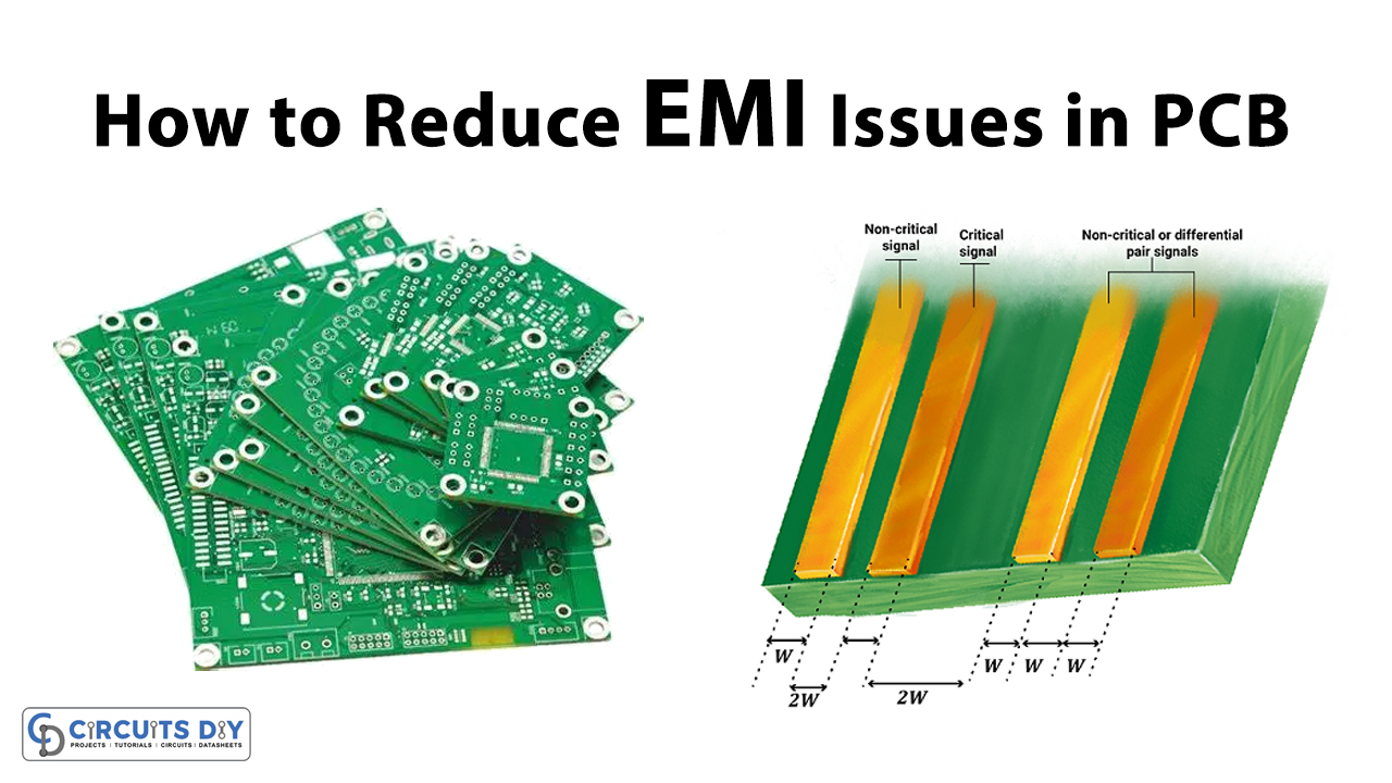
- Trace Spacing: Separate traces of different signals. Use the shunt and ground traces for clock lines. And, route differential traces closely.
- Best Use of Ground planes: to reduce EMI, use full ground planes. Hence, avoid the long paths. Remember, to avoid the copper fill areas
- Use of Cable Shielding: Cables carry digital and analog signals that may have parasitic capacitances. This can increase the EMI issues on the PCB. Therefore, use the cable shielding to avoid this.
- Utilize the Decoupling Capacitors: To reduce the power rail noise in the circuit, use the decoupling capacitors. Also, connect ground capacitors to the ground planes
- Control the Impedance: The impedance of the transmission line depend on numerous factors. That is the speed, an RF energy, and also the material of PCB. by controlling these factors the impedance can get controlled.

