Introduction
In this Tutorial, we will discuss the “NE5532 Dual Low Noise Op-amp Datasheet”. Because of its noise immunity and high output drive capabilities, the NE5532 Dual Low Noise Op-Amp is often employed as an amplifier in audio circuits. Internal compensation is used to provide a high unity gain with a wide output swing bandwidth, minimal distortion, and a fast slew rate.
Features of NE5532
- Equivalent Input Noise Voltage: 5 nV/√Hz at 1 kHz
- Unity-Gain Bandwidth: 10 MHz
- Common-Mode Rejection ratio:100 dB
- High dc Voltage Gain: 100 V/mV
- Peak-to-Peak Output Voltage Swing: 32 V With VCC± = ±18 V and RL = 600 ΩD
- High Slew Rate: 9 V/μs
- Wide Supply-Voltage Range: ±3 V to±20 V
NE5532 Pinout
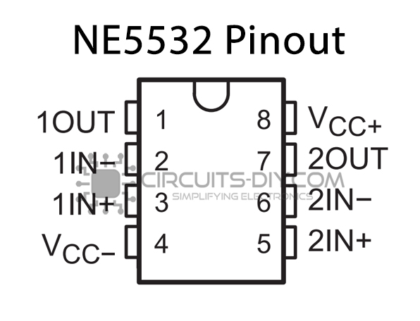
| Pin Number | Name | Description |
| 1 | 1 OUT | The output of Op-Amp A |
| 2 | 1 IN- | Inverting Input of Op-Amp A |
| 3 | 1 IN + | Non-Inverting Input of Op-Amp A |
| 4 | Vcc- | Ground or Negative Supply Voltage |
| 5 | 2 IN + | Non-Inverting Input of Op-Amp B |
| 6 | 2 IN – | Inverting Input of Op-Amp B |
| 7 | 2OUT | The output of Op-Amp B |
| 8 | VCC+ | Positive Supply Voltage |
Simple Preamplifier Circuit NE5532
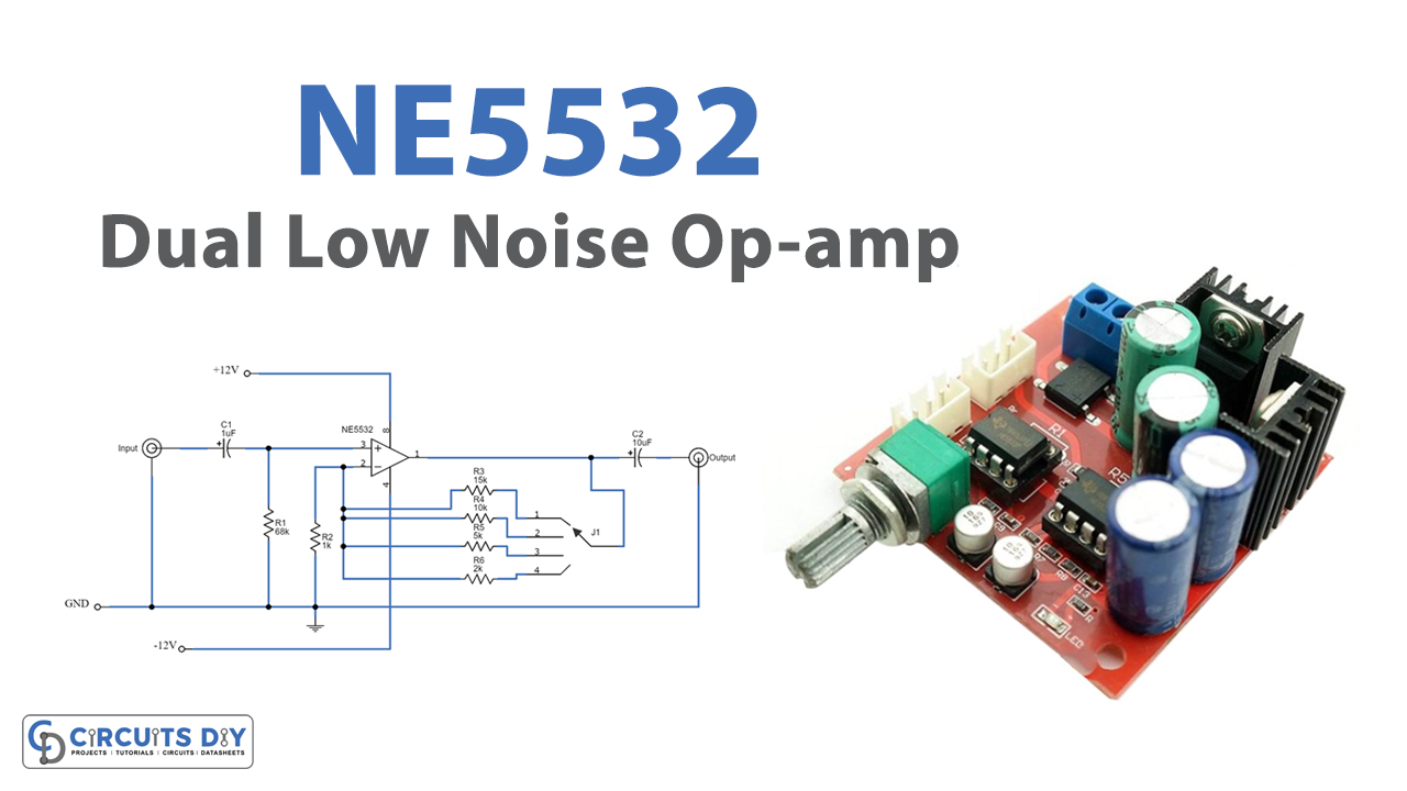
To understand the working of NE5532 IC, let’s make a simple preamplifier circuit.
Hardware Required
Circuit Diagram
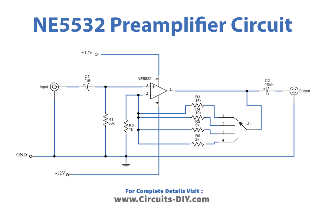
Working Explanation
In this preamplifier circuit, we provide the audio at pin 3 f an Ic, which is the noninverting pin of an IC. While the output is coming from pin 1. Where the switch is connected. Different growth rates can be selected by twisting the selection switch.
Application Uses
- Amplifiers in audio circuits
- Tone control circuit
- Graphic equalizer circuit

