The LF398 is a monolithic sample-and-hold circuit that utilizes BI-FET technology to obtain ultra-high dc accuracy with fast acquisition of signal and low droop rate. Operating as a unity gain follower, dc gain accuracy is 0.002% typical and acquisition time is as low as 6 µs to 0.01%. A bipolar input stage is used to achieve low offset voltage and wide bandwidth. Input offset adjustment is accomplished with a single pin and does not degrade input offset drift. The wide bandwidth allows the LF198 to be included inside the feedback loop of 1 MHz op amps without having stability problems.
The input impedance of 1010Ω allows high source impedances to be used without degrading accuracy. P-channel junction FET is combined with bipolar devices in the output amplifier to give droop rates as low as 5 mV/min with a 1 µF hold capacitor. The JFETs have much lower noise than MOS devices used in previous designs and do not exhibit high-temperature instabilities. The overall design guarantees no feed-through from input to output in the hold mode, even for input signals equal to the supply voltages.
LF398 Pinout
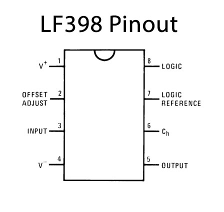
LF398 Pin Configuration
| Pin No | Pin Name | Description |
|---|---|---|
| 1 | V+ | Positive Supply Voltage |
| 2 | OFFSET ADJUST | Offset Adjust Pin |
| 3 | IN | Input Pin |
| 4 | V- | Negative Supply Voltage |
| 5 | OUT | Output Pin |
| 6 | CH | Channel Pin |
| 7 | Logic REF: | Logic Reference Pin |
| 8 | LOGIC | Logic Pin |
LF398 Features
- Operates from ±5V to ±18V supplies
- Less than 10 µs acquisition time
- TTL, PMOS, CMOS compatible logic input
- 0.5 mV typical hold step at Ch = 0.01 µF
- Low input offset
- 0.002% gain accuracy
- Low output noise in hold mode
- Input characteristics do not change during hold mode
- High supply rejection ratio in sample or hold
- Wide bandwidth
Application
- Ramp Generator
- Analog Switches
- Staircase Generator
- Sample and Difference Circuits
You can download this datasheet for LF398 Sample and Hold Circuit – Datasheet from the link given below: