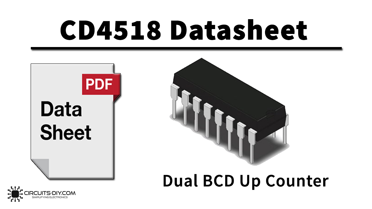
CD4518 Dual BCD Up Counter consists of two identical, internally synchronous 4-stage counters. The counter stages are D-type flip-flops having interchangeable CLK and EN lines for incrementing on either the positive going or negative going transition. The IC also offers many features such as high noise immunity and low thermal dissipation. The IC is always available in 16 – pin hermetically sealed package and is directly interfaceable with every TTL, CMOS & NMOS device. . The counter can be cascaded in the ripple mode by connecting Q4 to the enable input of the subsequent counter while the CLOCK input of the latter is held low.

What is A BCD Up Counter?
A binary coded decimal (BCD) Up Counter consists of four synchronously clocked D-type flip-flops connected as a counter. It can either count up from zero to nine. The output of a BCD counter is always indicated in binary format. It goes through 10 unique combinations of output & RESETS for every new clock input. A BCD counter can count 0000, 0001, 0010, 1000, 1001, 1010, 1011, 1110, 1111, 0000, and 0001 and so on.
CD4518 Key Features
- High Voltage Types (20V Rating)
- CD4518BMS Dual BCD Up Counter
- CD4520BMS Dual Binary Up Counter
- Medium Speed Operation
- 6MHz Typical Clock Frequency at 10V
- Positive or Negative Edge Triggering
- Synchronous Internal Carry Propagation
- 100% Tested for Quiescent Current at 20V
- 5V, 10V and 15V Parametric Ratings
- Maximum Input Current of 1µA at 18V Over Full Package Temperature Range; 100nA at 18V and +25oC
- Noise Margin (Over Full Package/Temperature Range)
- 1V at VDD = 5V
- 2V at VDD = 10V
- 2.5V at VDD = 15V
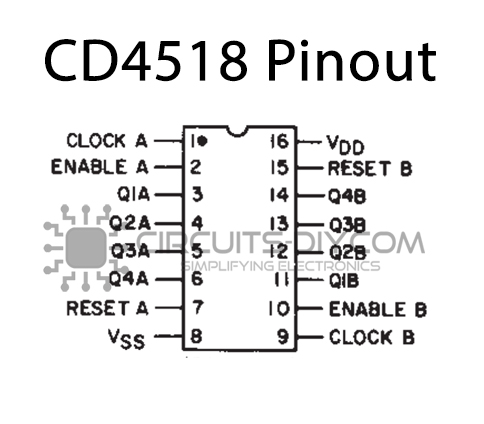
CD4518 Pinout
| Pin No | Pin Name | Description |
|---|---|---|
| 1 | CLOCK A | clock pin of counter A |
| 2 | ENABLE A | enable pin of counter A |
| 3 | Q1A | output pin 1 of counter A |
| 4 | Q2A | output pin 2 of counter A |
| 5 | Q3A | output pin 3 of counter A |
| 6 | Q4A | output pin 4 of counter A |
| 7 | RESET A | reset pin of counter A |
| 8 | VSS | source supply |
| 9 | ENABLE B | enable pin of counter B |
| 10 | CLOCK B | clock pin of counter B |
| 11 | Q1B | output pin 1 of counter B |
| 12 | Q2B | output pin 2 of counter B |
| 13 | Q3B | output pin 3 of counter B |
| 14 | Q4B | output pin 4 of counter B |
| 15 | RESET B | reset pin of counter B |
| 16 | VDD | drain supply |
Application
- Multistage Synchronous Counting
- Multistage Ripple Counting
- Frequency Dividers
CD4518 Datasheet
You can download the datasheet for CD4518 Dual BCD Up Counter from the link given below:
See Also: CD4001 Quad 2-input NOR Gate – Datasheet | CD4556 Dual Binary 1 of 4 Decoder Inverter – Datasheet | CD4521 24-Stage Frequency Divider – Datasheet

